0
U.S. (TOLL FREE)
+1 (315) 215-3225
Automative

0
U.S. (TOLL FREE)
+1 (315) 215-3225
Global SiC & GaN Wafer Defect Inspection System Market Research Report 2025
Published Date: June 2025
|
Report Code: QYRE-Auto-11M17816
Home | Market Reports | Computers & Electronics| Electronics & Electrical
Global SiC GaN Wafer Defect Inspection System Market Research Report 2024
BUY CHAPTERS

Global SiC & GaN Wafer Defect Inspection System Market Research Report 2025

Code: QYRE-Auto-11M17816
Report
June 2025
Pages:113
QYResearch
Buy Now with 15% Discount
DESCRIPTION
TABLE OF CONTENT
TABLES & FIGURES

SiC & GaN Wafer Defect Inspection System Market Size

The global market for SiC & GaN Wafer Defect Inspection System was valued at US$ 1042 million in the year 2024 and is projected to reach a revised size of US$ 3452 million by 2031, growing at a CAGR of 18.9% during the forecast period.

SiC & GaN Wafer Defect Inspection System Market

SiC & GaN Wafer Defect Inspection System Market

Inspection and metrology are becoming more critical in the silicon carbide (SiC) industry amid a pressing need to find problematic defects in current and future SiC devices. Finding defects always has been a challenging task for SiC devices. But it's becoming more imperative to find killer defects and reduce them as SiC device vendors begin to expand their production for the next wave of applications, particularly battery-electric vehicles. So SiC device makers will need to bolster their process control measures with more inspection and metrology in the fab. Fortunately, the inspection and metrology equipment for SiC has recently become available, but these tools add cost to the fab equation. Generally, inspection systems locate defects on the wafer, while metrology tools characterize the structures in devices. Both technologies are used to pinpoint problems and ensure yields for all chip types. SiC, a compound semiconductor material based on silicon and carbon, is used to make specialized power semiconductors for high-voltage applications, such as electric vehicles, power supplies and solar inverters. SiC has several advantages over conventional silicon-based power semis like IGBTs and power MOSFETs. But the silicon-based solutions dominate the market because they are less expensive than SiC. In recent times, SiC device makers completed a difficult transition from 100mm (4-inch) to 150mm (6-inch) wafers to 200mm (8-inch) in the fab. Some vendors, though, are still struggling with their yields and defect levels at 150mm. A few vendors have overcome most of these challenges, however. Amid the challenges in the market, SiC device makers are now seeing an increase in demand for battery-electric cars. For years, SiC vendors have served the automotive market to a limited degree. But for next-generation electric vehicles, the industry will need to bring the technology to the next level and meet the industry's rigid reliability, defect and cost specs.
Global key players of SiC Wafer Defect Inspection System include KLA Corporation, Lasertec, Bruker, Visiontec Group, TASMIT, Inc., etc. The top five players hold a share about 95%. North America is the largest market, and has a share about 32%, followed by Europe and Japan with share 27% and 15%, separately. In terms of product type, Optical Inspection System is the largest segment, occupied for a share of 97%. In terms of application, SiC Substrate has a share about 73 percent.

Report Scope

This report aims to provide a comprehensive presentation of the global market for SiC & GaN Wafer Defect Inspection System, with both quantitative and qualitative analysis, to help readers develop business/growth strategies, assess the market competitive situation, analyze their position in the current marketplace, and make informed business decisions regarding SiC & GaN Wafer Defect Inspection System.
The SiC & GaN Wafer Defect Inspection System market size, estimations, and forecasts are provided in terms of output/shipments (Units) and revenue ($ millions), considering 2024 as the base year, with history and forecast data for the period from 2020 to 2031. This report segments the global SiC & GaN Wafer Defect Inspection System market comprehensively. Regional market sizes, concerning products by Type, by Application, and by players, are also provided.
For a more in-depth understanding of the market, the report provides profiles of the competitive landscape, key competitors, and their respective market ranks. The report also discusses technological trends and new product developments.
The report will help the SiC & GaN Wafer Defect Inspection System manufacturers, new entrants, and industry chain related companies in this market with information on the revenues, production, and average price for the overall market and the sub-segments across the different segments, by company, by Type, by Application, and by regions.
Market Segmentation

Scope of SiC & GaN Wafer Defect Inspection System Market Report

Report Metric Details
Report Name SiC & GaN Wafer Defect Inspection System Market
Accounted market size in year US$ 1042 million
Forecasted market size in 2031 US$ 3452 million
CAGR 18.9%
Base Year year
Forecasted years 2025 - 2031
by Type
  • Optical Inspection System
  • X-ray Diffraction Imaging (XRDI) System
by Application
  • SiC Substrate, Epitaxy and Devices
  • GaN Substrate, Epitaxy and Devices
Production by Region
  • North America
  • China
  • Japan
  • South Korea
  • China Taiwan
  • Singapore
Consumption by Region
  • North America (United States, Canada)
  • Europe (Germany, France, UK, Italy, Russia)
  • Asia-Pacific (China, Japan, South Korea, Taiwan)
  • Southeast Asia (India)
  • Latin America (Mexico, Brazil)
By Company KLA Corporation, Lasertec, Visiontec Group, Nanotronics, TASMIT, Inc., Bruker, LAZIN CO.,LTD, EtaMax, Spirox Corporation, Angkun Vision (Beijing) Technology, Shenzhen Glint Vision, CETC Fenghua Information Equipment, CASI Vision Technology (Luoyang) Co., Ltd, Shanghai Youruipu Semiconductor Equipment, Dalian Chuangrui Spectral Technology Co., Ltd, T-Vision.AI (Hangzhou) Tech Co.,Ltd., HGTECH
Forecast units USD million in value
Report coverage Revenue and volume forecast, company share, competitive landscape, growth factors and trends

Chapter Outline

  • Chapter 1: Introduces the report scope of the report, executive summary of different market segments (by region, by Type, by Application, etc), including the market size of each market segment, future development potential, and so on. It offers a high-level view of the current state of the market and its likely evolution in the short to mid-term, and long term.
  • Chapter 2: Detailed analysis of SiC & GaN Wafer Defect Inspection System manufacturers competitive landscape, price, production and value market share, latest development plan, merger, and acquisition information, etc.
  • Chapter 3: Production/output, value of SiC & GaN Wafer Defect Inspection System by region/country. It provides a quantitative analysis of the market size and development potential of each region in the next six years.
  • Chapter 4: Consumption of SiC & GaN Wafer Defect Inspection System in regional level and country level. It provides a quantitative analysis of the market size and development potential of each region and its main countries and introduces the market development, future development prospects, market space, and production of each country in the world.
  • Chapter 5: Provides the analysis of various market segments by Type, covering the market size and development potential of each market segment, to help readers find the blue ocean market in different market segments.
  • Chapter 6: Provides the analysis of various market segments by Application, covering the market size and development potential of each market segment, to help readers find the blue ocean market in different downstream markets.
  • Chapter 7: Provides profiles of key players, introducing the basic situation of the main companies in the market in detail, including product production/output, value, price, gross margin, product introduction, recent development, etc.
  • Chapter 8: Analysis of industrial chain, including the upstream and downstream of the industry.
  • Chapter 9: Introduces the market dynamics, latest developments of the market, the driving factors and restrictive factors of the market, the challenges and risks faced by manufacturers in the industry, and the analysis of relevant policies in the industry.
  • Chapter 10: The main points and conclusions of the report.

FAQ for this report

How fast is SiC & GaN Wafer Defect Inspection System Market growing?

Ans: The SiC & GaN Wafer Defect Inspection System Market witnessing a CAGR of 18.9% during the forecast period 2025-2031.

What is the SiC & GaN Wafer Defect Inspection System Market size in 2031?

Ans: The SiC & GaN Wafer Defect Inspection System Market size in 2031 will be US$ 3452 million.

What is the market share of major companies in SiC & GaN Wafer Defect Inspection System Market?

Ans: The top five players hold a share about 95%.

What is the SiC & GaN Wafer Defect Inspection System Market share by region?

Ans: North America is the largest market, and has a share about 32%, followed by Europe and Japan with share 27% and 15%, separately.

What is the SiC & GaN Wafer Defect Inspection System Market share by type?

Ans: In terms of product type, Optical Inspection System is the largest segment, occupied for a share of 97%.

Who are the main players in the SiC & GaN Wafer Defect Inspection System Market report?

Ans: The main players in the SiC & GaN Wafer Defect Inspection System Market are KLA Corporation, Lasertec, Visiontec Group, Nanotronics, TASMIT, Inc., Bruker, LAZIN CO.,LTD, EtaMax, Spirox Corporation, Angkun Vision (Beijing) Technology, Shenzhen Glint Vision, CETC Fenghua Information Equipment, CASI Vision Technology (Luoyang) Co., Ltd, Shanghai Youruipu Semiconductor Equipment, Dalian Chuangrui Spectral Technology Co., Ltd, T-Vision.AI (Hangzhou) Tech Co.,Ltd., HGTECH

What are the Application segmentation covered in the SiC & GaN Wafer Defect Inspection System Market report?

Ans: The Applications covered in the SiC & GaN Wafer Defect Inspection System Market report are SiC Substrate, Epitaxy and Devices, GaN Substrate, Epitaxy and Devices

What are the Type segmentation covered in the SiC & GaN Wafer Defect Inspection System Market report?

Ans: The Types covered in the SiC & GaN Wafer Defect Inspection System Market report are Optical Inspection System, X-ray Diffraction Imaging (XRDI) System

1 SiC & GaN Wafer Defect Inspection System Market Overview
1.1 Product Definition
1.2 SiC & GaN Wafer Defect Inspection System by Type
1.2.1 Global SiC & GaN Wafer Defect Inspection System Market Value Growth Rate Analysis by Type: 2024 VS 2031
1.2.2 Optical Inspection System
1.2.3 X-ray Diffraction Imaging (XRDI) System
1.3 SiC & GaN Wafer Defect Inspection System by Application
1.3.1 Global SiC & GaN Wafer Defect Inspection System Market Value Growth Rate Analysis by Application: 2024 VS 2031
1.3.2 SiC Substrate, Epitaxy and Devices
1.3.3 GaN Substrate, Epitaxy and Devices
1.4 Global Market Growth Prospects
1.4.1 Global SiC & GaN Wafer Defect Inspection System Production Value Estimates and Forecasts (2020-2031)
1.4.2 Global SiC & GaN Wafer Defect Inspection System Production Capacity Estimates and Forecasts (2020-2031)
1.4.3 Global SiC & GaN Wafer Defect Inspection System Production Estimates and Forecasts (2020-2031)
1.4.4 Global SiC & GaN Wafer Defect Inspection System Market Average Price Estimates and Forecasts (2020-2031)
1.5 Assumptions and Limitations
2 Market Competition by Manufacturers
2.1 Global SiC & GaN Wafer Defect Inspection System Production Market Share by Manufacturers (2020-2025)
2.2 Global SiC & GaN Wafer Defect Inspection System Production Value Market Share by Manufacturers (2020-2025)
2.3 Global Key Players of SiC & GaN Wafer Defect Inspection System, Industry Ranking, 2023 VS 2024
2.4 Global SiC & GaN Wafer Defect Inspection System Market Share by Company Type (Tier 1, Tier 2, and Tier 3)
2.5 Global SiC & GaN Wafer Defect Inspection System Average Price by Manufacturers (2020-2025)
2.6 Global Key Manufacturers of SiC & GaN Wafer Defect Inspection System, Manufacturing Base Distribution and Headquarters
2.7 Global Key Manufacturers of SiC & GaN Wafer Defect Inspection System, Product Offered and Application
2.8 Global Key Manufacturers of SiC & GaN Wafer Defect Inspection System, Date of Enter into This Industry
2.9 SiC & GaN Wafer Defect Inspection System Market Competitive Situation and Trends
2.9.1 SiC & GaN Wafer Defect Inspection System Market Concentration Rate
2.9.2 Global 5 and 10 Largest SiC & GaN Wafer Defect Inspection System Players Market Share by Revenue
2.10 Mergers & Acquisitions, Expansion
3 SiC & GaN Wafer Defect Inspection System Production by Region
3.1 Global SiC & GaN Wafer Defect Inspection System Production Value Estimates and Forecasts by Region: 2020 VS 2024 VS 2031
3.2 Global SiC & GaN Wafer Defect Inspection System Production Value by Region (2020-2031)
3.2.1 Global SiC & GaN Wafer Defect Inspection System Production Value by Region (2020-2025)
3.2.2 Global Forecasted Production Value of SiC & GaN Wafer Defect Inspection System by Region (2026-2031)
3.3 Global SiC & GaN Wafer Defect Inspection System Production Estimates and Forecasts by Region: 2020 VS 2024 VS 2031
3.4 Global SiC & GaN Wafer Defect Inspection System Production Volume by Region (2020-2031)
3.4.1 Global SiC & GaN Wafer Defect Inspection System Production by Region (2020-2025)
3.4.2 Global Forecasted Production of SiC & GaN Wafer Defect Inspection System by Region (2026-2031)
3.5 Global SiC & GaN Wafer Defect Inspection System Market Price Analysis by Region (2020-2025)
3.6 Global SiC & GaN Wafer Defect Inspection System Production and Value, Year-over-Year Growth
3.6.1 North America SiC & GaN Wafer Defect Inspection System Production Value Estimates and Forecasts (2020-2031)
3.6.2 China SiC & GaN Wafer Defect Inspection System Production Value Estimates and Forecasts (2020-2031)
3.6.3 Japan SiC & GaN Wafer Defect Inspection System Production Value Estimates and Forecasts (2020-2031)
3.6.4 South Korea SiC & GaN Wafer Defect Inspection System Production Value Estimates and Forecasts (2020-2031)
3.6.5 China Taiwan SiC & GaN Wafer Defect Inspection System Production Value Estimates and Forecasts (2020-2031)
3.6.6 Singapore SiC & GaN Wafer Defect Inspection System Production Value Estimates and Forecasts (2020-2031)
4 SiC & GaN Wafer Defect Inspection System Consumption by Region
4.1 Global SiC & GaN Wafer Defect Inspection System Consumption Estimates and Forecasts by Region: 2020 VS 2024 VS 2031
4.2 Global SiC & GaN Wafer Defect Inspection System Consumption by Region (2020-2031)
4.2.1 Global SiC & GaN Wafer Defect Inspection System Consumption by Region (2020-2025)
4.2.2 Global SiC & GaN Wafer Defect Inspection System Forecasted Consumption by Region (2026-2031)
4.3 North America
4.3.1 North America SiC & GaN Wafer Defect Inspection System Consumption Growth Rate by Country: 2020 VS 2024 VS 2031
4.3.2 North America SiC & GaN Wafer Defect Inspection System Consumption by Country (2020-2031)
4.3.3 U.S.
4.3.4 Canada
4.4 Europe
4.4.1 Europe SiC & GaN Wafer Defect Inspection System Consumption Growth Rate by Country: 2020 VS 2024 VS 2031
4.4.2 Europe SiC & GaN Wafer Defect Inspection System Consumption by Country (2020-2031)
4.4.3 Germany
4.4.4 France
4.4.5 U.K.
4.4.6 Italy
4.4.7 Netherlands
4.5 Asia Pacific
4.5.1 Asia Pacific SiC & GaN Wafer Defect Inspection System Consumption Growth Rate by Region: 2020 VS 2024 VS 2031
4.5.2 Asia Pacific SiC & GaN Wafer Defect Inspection System Consumption by Region (2020-2031)
4.5.3 China
4.5.4 Japan
4.5.5 South Korea
4.5.6 China Taiwan
4.5.7 Southeast Asia
4.5.8 India
4.6 Latin America, Middle East & Africa
4.6.1 Latin America, Middle East & Africa SiC & GaN Wafer Defect Inspection System Consumption Growth Rate by Country: 2020 VS 2024 VS 2031
4.6.2 Latin America, Middle East & Africa SiC & GaN Wafer Defect Inspection System Consumption by Country (2020-2031)
4.6.3 Mexico
4.6.4 Brazil
4.6.5 Israel
5 Segment by Type
5.1 Global SiC & GaN Wafer Defect Inspection System Production by Type (2020-2031)
5.1.1 Global SiC & GaN Wafer Defect Inspection System Production by Type (2020-2025)
5.1.2 Global SiC & GaN Wafer Defect Inspection System Production by Type (2026-2031)
5.1.3 Global SiC & GaN Wafer Defect Inspection System Production Market Share by Type (2020-2031)
5.2 Global SiC & GaN Wafer Defect Inspection System Production Value by Type (2020-2031)
5.2.1 Global SiC & GaN Wafer Defect Inspection System Production Value by Type (2020-2025)
5.2.2 Global SiC & GaN Wafer Defect Inspection System Production Value by Type (2026-2031)
5.2.3 Global SiC & GaN Wafer Defect Inspection System Production Value Market Share by Type (2020-2031)
5.3 Global SiC & GaN Wafer Defect Inspection System Price by Type (2020-2031)
6 Segment by Application
6.1 Global SiC & GaN Wafer Defect Inspection System Production by Application (2020-2031)
6.1.1 Global SiC & GaN Wafer Defect Inspection System Production by Application (2020-2025)
6.1.2 Global SiC & GaN Wafer Defect Inspection System Production by Application (2026-2031)
6.1.3 Global SiC & GaN Wafer Defect Inspection System Production Market Share by Application (2020-2031)
6.2 Global SiC & GaN Wafer Defect Inspection System Production Value by Application (2020-2031)
6.2.1 Global SiC & GaN Wafer Defect Inspection System Production Value by Application (2020-2025)
6.2.2 Global SiC & GaN Wafer Defect Inspection System Production Value by Application (2026-2031)
6.2.3 Global SiC & GaN Wafer Defect Inspection System Production Value Market Share by Application (2020-2031)
6.3 Global SiC & GaN Wafer Defect Inspection System Price by Application (2020-2031)
7 Key Companies Profiled
7.1 KLA Corporation
7.1.1 KLA Corporation SiC & GaN Wafer Defect Inspection System Company Information
7.1.2 KLA Corporation SiC & GaN Wafer Defect Inspection System Product Portfolio
7.1.3 KLA Corporation SiC & GaN Wafer Defect Inspection System Production, Value, Price and Gross Margin (2020-2025)
7.1.4 KLA Corporation Main Business and Markets Served
7.1.5 KLA Corporation Recent Developments/Updates
7.2 Lasertec
7.2.1 Lasertec SiC & GaN Wafer Defect Inspection System Company Information
7.2.2 Lasertec SiC & GaN Wafer Defect Inspection System Product Portfolio
7.2.3 Lasertec SiC & GaN Wafer Defect Inspection System Production, Value, Price and Gross Margin (2020-2025)
7.2.4 Lasertec Main Business and Markets Served
7.2.5 Lasertec Recent Developments/Updates
7.3 Visiontec Group
7.3.1 Visiontec Group SiC & GaN Wafer Defect Inspection System Company Information
7.3.2 Visiontec Group SiC & GaN Wafer Defect Inspection System Product Portfolio
7.3.3 Visiontec Group SiC & GaN Wafer Defect Inspection System Production, Value, Price and Gross Margin (2020-2025)
7.3.4 Visiontec Group Main Business and Markets Served
7.3.5 Visiontec Group Recent Developments/Updates
7.4 Nanotronics
7.4.1 Nanotronics SiC & GaN Wafer Defect Inspection System Company Information
7.4.2 Nanotronics SiC & GaN Wafer Defect Inspection System Product Portfolio
7.4.3 Nanotronics SiC & GaN Wafer Defect Inspection System Production, Value, Price and Gross Margin (2020-2025)
7.4.4 Nanotronics Main Business and Markets Served
7.4.5 Nanotronics Recent Developments/Updates
7.5 TASMIT, Inc.
7.5.1 TASMIT, Inc. SiC & GaN Wafer Defect Inspection System Company Information
7.5.2 TASMIT, Inc. SiC & GaN Wafer Defect Inspection System Product Portfolio
7.5.3 TASMIT, Inc. SiC & GaN Wafer Defect Inspection System Production, Value, Price and Gross Margin (2020-2025)
7.5.4 TASMIT, Inc. Main Business and Markets Served
7.5.5 TASMIT, Inc. Recent Developments/Updates
7.6 Bruker
7.6.1 Bruker SiC & GaN Wafer Defect Inspection System Company Information
7.6.2 Bruker SiC & GaN Wafer Defect Inspection System Product Portfolio
7.6.3 Bruker SiC & GaN Wafer Defect Inspection System Production, Value, Price and Gross Margin (2020-2025)
7.6.4 Bruker Main Business and Markets Served
7.6.5 Bruker Recent Developments/Updates
7.7 LAZIN CO.,LTD
7.7.1 LAZIN CO.,LTD SiC & GaN Wafer Defect Inspection System Company Information
7.7.2 LAZIN CO.,LTD SiC & GaN Wafer Defect Inspection System Product Portfolio
7.7.3 LAZIN CO.,LTD SiC & GaN Wafer Defect Inspection System Production, Value, Price and Gross Margin (2020-2025)
7.7.4 LAZIN CO.,LTD Main Business and Markets Served
7.7.5 LAZIN CO.,LTD Recent Developments/Updates
7.8 EtaMax
7.8.1 EtaMax SiC & GaN Wafer Defect Inspection System Company Information
7.8.2 EtaMax SiC & GaN Wafer Defect Inspection System Product Portfolio
7.8.3 EtaMax SiC & GaN Wafer Defect Inspection System Production, Value, Price and Gross Margin (2020-2025)
7.8.4 EtaMax Main Business and Markets Served
7.8.5 EtaMax Recent Developments/Updates
7.9 Spirox Corporation
7.9.1 Spirox Corporation SiC & GaN Wafer Defect Inspection System Company Information
7.9.2 Spirox Corporation SiC & GaN Wafer Defect Inspection System Product Portfolio
7.9.3 Spirox Corporation SiC & GaN Wafer Defect Inspection System Production, Value, Price and Gross Margin (2020-2025)
7.9.4 Spirox Corporation Main Business and Markets Served
7.9.5 Spirox Corporation Recent Developments/Updates
7.10 Angkun Vision (Beijing) Technology
7.10.1 Angkun Vision (Beijing) Technology SiC & GaN Wafer Defect Inspection System Company Information
7.10.2 Angkun Vision (Beijing) Technology SiC & GaN Wafer Defect Inspection System Product Portfolio
7.10.3 Angkun Vision (Beijing) Technology SiC & GaN Wafer Defect Inspection System Production, Value, Price and Gross Margin (2020-2025)
7.10.4 Angkun Vision (Beijing) Technology Main Business and Markets Served
7.10.5 Angkun Vision (Beijing) Technology Recent Developments/Updates
7.11 Shenzhen Glint Vision
7.11.1 Shenzhen Glint Vision SiC & GaN Wafer Defect Inspection System Company Information
7.11.2 Shenzhen Glint Vision SiC & GaN Wafer Defect Inspection System Product Portfolio
7.11.3 Shenzhen Glint Vision SiC & GaN Wafer Defect Inspection System Production, Value, Price and Gross Margin (2020-2025)
7.11.4 Shenzhen Glint Vision Main Business and Markets Served
7.11.5 Shenzhen Glint Vision Recent Developments/Updates
7.12 CETC Fenghua Information Equipment
7.12.1 CETC Fenghua Information Equipment SiC & GaN Wafer Defect Inspection System Company Information
7.12.2 CETC Fenghua Information Equipment SiC & GaN Wafer Defect Inspection System Product Portfolio
7.12.3 CETC Fenghua Information Equipment SiC & GaN Wafer Defect Inspection System Production, Value, Price and Gross Margin (2020-2025)
7.12.4 CETC Fenghua Information Equipment Main Business and Markets Served
7.12.5 CETC Fenghua Information Equipment Recent Developments/Updates
7.13 CASI Vision Technology (Luoyang) Co., Ltd
7.13.1 CASI Vision Technology (Luoyang) Co., Ltd SiC & GaN Wafer Defect Inspection System Company Information
7.13.2 CASI Vision Technology (Luoyang) Co., Ltd SiC & GaN Wafer Defect Inspection System Product Portfolio
7.13.3 CASI Vision Technology (Luoyang) Co., Ltd SiC & GaN Wafer Defect Inspection System Production, Value, Price and Gross Margin (2020-2025)
7.13.4 CASI Vision Technology (Luoyang) Co., Ltd Main Business and Markets Served
7.13.5 CASI Vision Technology (Luoyang) Co., Ltd Recent Developments/Updates
7.14 Shanghai Youruipu Semiconductor Equipment
7.14.1 Shanghai Youruipu Semiconductor Equipment SiC & GaN Wafer Defect Inspection System Company Information
7.14.2 Shanghai Youruipu Semiconductor Equipment SiC & GaN Wafer Defect Inspection System Product Portfolio
7.14.3 Shanghai Youruipu Semiconductor Equipment SiC & GaN Wafer Defect Inspection System Production, Value, Price and Gross Margin (2020-2025)
7.14.4 Shanghai Youruipu Semiconductor Equipment Main Business and Markets Served
7.14.5 Shanghai Youruipu Semiconductor Equipment Recent Developments/Updates
7.15 Dalian Chuangrui Spectral Technology Co., Ltd
7.15.1 Dalian Chuangrui Spectral Technology Co., Ltd SiC & GaN Wafer Defect Inspection System Company Information
7.15.2 Dalian Chuangrui Spectral Technology Co., Ltd SiC & GaN Wafer Defect Inspection System Product Portfolio
7.15.3 Dalian Chuangrui Spectral Technology Co., Ltd SiC & GaN Wafer Defect Inspection System Production, Value, Price and Gross Margin (2020-2025)
7.15.4 Dalian Chuangrui Spectral Technology Co., Ltd Main Business and Markets Served
7.15.5 Dalian Chuangrui Spectral Technology Co., Ltd Recent Developments/Updates
7.16 T-Vision.AI (Hangzhou) Tech Co.,Ltd.
7.16.1 T-Vision.AI (Hangzhou) Tech Co.,Ltd. SiC & GaN Wafer Defect Inspection System Company Information
7.16.2 T-Vision.AI (Hangzhou) Tech Co.,Ltd. SiC & GaN Wafer Defect Inspection System Product Portfolio
7.16.3 T-Vision.AI (Hangzhou) Tech Co.,Ltd. SiC & GaN Wafer Defect Inspection System Production, Value, Price and Gross Margin (2020-2025)
7.16.4 T-Vision.AI (Hangzhou) Tech Co.,Ltd. Main Business and Markets Served
7.16.5 T-Vision.AI (Hangzhou) Tech Co.,Ltd. Recent Developments/Updates
7.17 HGTECH
7.17.1 HGTECH SiC & GaN Wafer Defect Inspection System Company Information
7.17.2 HGTECH SiC & GaN Wafer Defect Inspection System Product Portfolio
7.17.3 HGTECH SiC & GaN Wafer Defect Inspection System Production, Value, Price and Gross Margin (2020-2025)
7.17.4 HGTECH Main Business and Markets Served
7.17.5 HGTECH Recent Developments/Updates
8 Industry Chain and Sales Channels Analysis
8.1 SiC & GaN Wafer Defect Inspection System Industry Chain Analysis
8.2 SiC & GaN Wafer Defect Inspection System Raw Material Supply Analysis
8.2.1 Key Raw Materials
8.2.2 Raw Materials Key Suppliers
8.3 SiC & GaN Wafer Defect Inspection System Production Mode & Process Analysis
8.4 SiC & GaN Wafer Defect Inspection System Sales and Marketing
8.4.1 SiC & GaN Wafer Defect Inspection System Sales Channels
8.4.2 SiC & GaN Wafer Defect Inspection System Distributors
8.5 SiC & GaN Wafer Defect Inspection System Customer Analysis
9 SiC & GaN Wafer Defect Inspection System Market Dynamics
9.1 SiC & GaN Wafer Defect Inspection System Industry Trends
9.2 SiC & GaN Wafer Defect Inspection System Market Drivers
9.3 SiC & GaN Wafer Defect Inspection System Market Challenges
9.4 SiC & GaN Wafer Defect Inspection System Market Restraints
10 Research Findings and Conclusion
11 Methodology and Data Source
11.1 Methodology/Research Approach
11.1.1 Research Programs/Design
11.1.2 Market Size Estimation
11.1.3 Market Breakdown and Data Triangulation
11.2 Data Source
11.2.1 Secondary Sources
11.2.2 Primary Sources
11.3 Author List
11.4 Disclaimer
List of Tables
 Table 1. Global SiC & GaN Wafer Defect Inspection System Market Value by Type, (US$ Million) & (2024 VS 2031)
 Table 2. Global SiC & GaN Wafer Defect Inspection System Market Value by Application, (US$ Million) & (2024 VS 2031)
 Table 3. Global SiC & GaN Wafer Defect Inspection System Production Capacity (Units) by Manufacturers in 2024
 Table 4. Global SiC & GaN Wafer Defect Inspection System Production by Manufacturers (2020-2025) & (Units)
 Table 5. Global SiC & GaN Wafer Defect Inspection System Production Market Share by Manufacturers (2020-2025)
 Table 6. Global SiC & GaN Wafer Defect Inspection System Production Value by Manufacturers (2020-2025) & (US$ Million)
 Table 7. Global SiC & GaN Wafer Defect Inspection System Production Value Share by Manufacturers (2020-2025)
 Table 8. Global Key Players of SiC & GaN Wafer Defect Inspection System, Industry Ranking, 2023 VS 2024
 Table 9. Company Type (Tier 1, Tier 2, and Tier 3) & (based on the Production Value in SiC & GaN Wafer Defect Inspection System as of 2024)
 Table 10. Global Market SiC & GaN Wafer Defect Inspection System Average Price by Manufacturers (K US$/Unit) & (2020-2025)
 Table 11. Global Key Manufacturers of SiC & GaN Wafer Defect Inspection System, Manufacturing Base Distribution and Headquarters
 Table 12. Global Key Manufacturers of SiC & GaN Wafer Defect Inspection System, Product Offered and Application
 Table 13. Global Key Manufacturers of SiC & GaN Wafer Defect Inspection System, Date of Enter into This Industry
 Table 14. Global SiC & GaN Wafer Defect Inspection System Manufacturers Market Concentration Ratio (CR5 and HHI)
 Table 15. Mergers & Acquisitions, Expansion Plans
 Table 16. Global SiC & GaN Wafer Defect Inspection System Production Value by Region: 2020 VS 2024 VS 2031 (US$ Million)
 Table 17. Global SiC & GaN Wafer Defect Inspection System Production Value (US$ Million) by Region (2020-2025)
 Table 18. Global SiC & GaN Wafer Defect Inspection System Production Value Market Share by Region (2020-2025)
 Table 19. Global SiC & GaN Wafer Defect Inspection System Production Value (US$ Million) Forecast by Region (2026-2031)
 Table 20. Global SiC & GaN Wafer Defect Inspection System Production Value Market Share Forecast by Region (2026-2031)
 Table 21. Global SiC & GaN Wafer Defect Inspection System Production Comparison by Region: 2020 VS 2024 VS 2031 (Units)
 Table 22. Global SiC & GaN Wafer Defect Inspection System Production (Units) by Region (2020-2025)
 Table 23. Global SiC & GaN Wafer Defect Inspection System Production Market Share by Region (2020-2025)
 Table 24. Global SiC & GaN Wafer Defect Inspection System Production (Units) Forecast by Region (2026-2031)
 Table 25. Global SiC & GaN Wafer Defect Inspection System Production Market Share Forecast by Region (2026-2031)
 Table 26. Global SiC & GaN Wafer Defect Inspection System Market Average Price (K US$/Unit) by Region (2020-2025)
 Table 27. Global SiC & GaN Wafer Defect Inspection System Market Average Price (K US$/Unit) by Region (2026-2031)
 Table 28. Global SiC & GaN Wafer Defect Inspection System Consumption Growth Rate by Region: 2020 VS 2024 VS 2031 (Units)
 Table 29. Global SiC & GaN Wafer Defect Inspection System Consumption by Region (2020-2025) & (Units)
 Table 30. Global SiC & GaN Wafer Defect Inspection System Consumption Market Share by Region (2020-2025)
 Table 31. Global SiC & GaN Wafer Defect Inspection System Forecasted Consumption by Region (2026-2031) & (Units)
 Table 32. Global SiC & GaN Wafer Defect Inspection System Forecasted Consumption Market Share by Region (2026-2031)
 Table 33. North America SiC & GaN Wafer Defect Inspection System Consumption Growth Rate by Country: 2020 VS 2024 VS 2031 (Units)
 Table 34. North America SiC & GaN Wafer Defect Inspection System Consumption by Country (2020-2025) & (Units)
 Table 35. North America SiC & GaN Wafer Defect Inspection System Consumption by Country (2026-2031) & (Units)
 Table 36. Europe SiC & GaN Wafer Defect Inspection System Consumption Growth Rate by Country: 2020 VS 2024 VS 2031 (Units)
 Table 37. Europe SiC & GaN Wafer Defect Inspection System Consumption by Country (2020-2025) & (Units)
 Table 38. Europe SiC & GaN Wafer Defect Inspection System Consumption by Country (2026-2031) & (Units)
 Table 39. Asia Pacific SiC & GaN Wafer Defect Inspection System Consumption Growth Rate by Region: 2020 VS 2024 VS 2031 (Units)
 Table 40. Asia Pacific SiC & GaN Wafer Defect Inspection System Consumption by Region (2020-2025) & (Units)
 Table 41. Asia Pacific SiC & GaN Wafer Defect Inspection System Consumption by Region (2026-2031) & (Units)
 Table 42. Latin America, Middle East & Africa SiC & GaN Wafer Defect Inspection System Consumption Growth Rate by Country: 2020 VS 2024 VS 2031 (Units)
 Table 43. Latin America, Middle East & Africa SiC & GaN Wafer Defect Inspection System Consumption by Country (2020-2025) & (Units)
 Table 44. Latin America, Middle East & Africa SiC & GaN Wafer Defect Inspection System Consumption by Country (2026-2031) & (Units)
 Table 45. Global SiC & GaN Wafer Defect Inspection System Production (Units) by Type (2020-2025)
 Table 46. Global SiC & GaN Wafer Defect Inspection System Production (Units) by Type (2026-2031)
 Table 47. Global SiC & GaN Wafer Defect Inspection System Production Market Share by Type (2020-2025)
 Table 48. Global SiC & GaN Wafer Defect Inspection System Production Market Share by Type (2026-2031)
 Table 49. Global SiC & GaN Wafer Defect Inspection System Production Value (US$ Million) by Type (2020-2025)
 Table 50. Global SiC & GaN Wafer Defect Inspection System Production Value (US$ Million) by Type (2026-2031)
 Table 51. Global SiC & GaN Wafer Defect Inspection System Production Value Market Share by Type (2020-2025)
 Table 52. Global SiC & GaN Wafer Defect Inspection System Production Value Market Share by Type (2026-2031)
 Table 53. Global SiC & GaN Wafer Defect Inspection System Price (K US$/Unit) by Type (2020-2025)
 Table 54. Global SiC & GaN Wafer Defect Inspection System Price (K US$/Unit) by Type (2026-2031)
 Table 55. Global SiC & GaN Wafer Defect Inspection System Production (Units) by Application (2020-2025)
 Table 56. Global SiC & GaN Wafer Defect Inspection System Production (Units) by Application (2026-2031)
 Table 57. Global SiC & GaN Wafer Defect Inspection System Production Market Share by Application (2020-2025)
 Table 58. Global SiC & GaN Wafer Defect Inspection System Production Market Share by Application (2026-2031)
 Table 59. Global SiC & GaN Wafer Defect Inspection System Production Value (US$ Million) by Application (2020-2025)
 Table 60. Global SiC & GaN Wafer Defect Inspection System Production Value (US$ Million) by Application (2026-2031)
 Table 61. Global SiC & GaN Wafer Defect Inspection System Production Value Market Share by Application (2020-2025)
 Table 62. Global SiC & GaN Wafer Defect Inspection System Production Value Market Share by Application (2026-2031)
 Table 63. Global SiC & GaN Wafer Defect Inspection System Price (K US$/Unit) by Application (2020-2025)
 Table 64. Global SiC & GaN Wafer Defect Inspection System Price (K US$/Unit) by Application (2026-2031)
 Table 65. KLA Corporation SiC & GaN Wafer Defect Inspection System Company Information
 Table 66. KLA Corporation SiC & GaN Wafer Defect Inspection System Specification and Application
 Table 67. KLA Corporation SiC & GaN Wafer Defect Inspection System Production (Units), Value (US$ Million), Price (K US$/Unit) and Gross Margin (2020-2025)
 Table 68. KLA Corporation Main Business and Markets Served
 Table 69. KLA Corporation Recent Developments/Updates
 Table 70. Lasertec SiC & GaN Wafer Defect Inspection System Company Information
 Table 71. Lasertec SiC & GaN Wafer Defect Inspection System Specification and Application
 Table 72. Lasertec SiC & GaN Wafer Defect Inspection System Production (Units), Value (US$ Million), Price (K US$/Unit) and Gross Margin (2020-2025)
 Table 73. Lasertec Main Business and Markets Served
 Table 74. Lasertec Recent Developments/Updates
 Table 75. Visiontec Group SiC & GaN Wafer Defect Inspection System Company Information
 Table 76. Visiontec Group SiC & GaN Wafer Defect Inspection System Specification and Application
 Table 77. Visiontec Group SiC & GaN Wafer Defect Inspection System Production (Units), Value (US$ Million), Price (K US$/Unit) and Gross Margin (2020-2025)
 Table 78. Visiontec Group Main Business and Markets Served
 Table 79. Visiontec Group Recent Developments/Updates
 Table 80. Nanotronics SiC & GaN Wafer Defect Inspection System Company Information
 Table 81. Nanotronics SiC & GaN Wafer Defect Inspection System Specification and Application
 Table 82. Nanotronics SiC & GaN Wafer Defect Inspection System Production (Units), Value (US$ Million), Price (K US$/Unit) and Gross Margin (2020-2025)
 Table 83. Nanotronics Main Business and Markets Served
 Table 84. Nanotronics Recent Developments/Updates
 Table 85. TASMIT, Inc. SiC & GaN Wafer Defect Inspection System Company Information
 Table 86. TASMIT, Inc. SiC & GaN Wafer Defect Inspection System Specification and Application
 Table 87. TASMIT, Inc. SiC & GaN Wafer Defect Inspection System Production (Units), Value (US$ Million), Price (K US$/Unit) and Gross Margin (2020-2025)
 Table 88. TASMIT, Inc. Main Business and Markets Served
 Table 89. TASMIT, Inc. Recent Developments/Updates
 Table 90. Bruker SiC & GaN Wafer Defect Inspection System Company Information
 Table 91. Bruker SiC & GaN Wafer Defect Inspection System Specification and Application
 Table 92. Bruker SiC & GaN Wafer Defect Inspection System Production (Units), Value (US$ Million), Price (K US$/Unit) and Gross Margin (2020-2025)
 Table 93. Bruker Main Business and Markets Served
 Table 94. Bruker Recent Developments/Updates
 Table 95. LAZIN CO.,LTD SiC & GaN Wafer Defect Inspection System Company Information
 Table 96. LAZIN CO.,LTD SiC & GaN Wafer Defect Inspection System Specification and Application
 Table 97. LAZIN CO.,LTD SiC & GaN Wafer Defect Inspection System Production (Units), Value (US$ Million), Price (K US$/Unit) and Gross Margin (2020-2025)
 Table 98. LAZIN CO.,LTD Main Business and Markets Served
 Table 99. LAZIN CO.,LTD Recent Developments/Updates
 Table 100. EtaMax SiC & GaN Wafer Defect Inspection System Company Information
 Table 101. EtaMax SiC & GaN Wafer Defect Inspection System Specification and Application
 Table 102. EtaMax SiC & GaN Wafer Defect Inspection System Production (Units), Value (US$ Million), Price (K US$/Unit) and Gross Margin (2020-2025)
 Table 103. EtaMax Main Business and Markets Served
 Table 104. EtaMax Recent Developments/Updates
 Table 105. Spirox Corporation SiC & GaN Wafer Defect Inspection System Company Information
 Table 106. Spirox Corporation SiC & GaN Wafer Defect Inspection System Specification and Application
 Table 107. Spirox Corporation SiC & GaN Wafer Defect Inspection System Production (Units), Value (US$ Million), Price (K US$/Unit) and Gross Margin (2020-2025)
 Table 108. Spirox Corporation Main Business and Markets Served
 Table 109. Spirox Corporation Recent Developments/Updates
 Table 110. Angkun Vision (Beijing) Technology SiC & GaN Wafer Defect Inspection System Company Information
 Table 111. Angkun Vision (Beijing) Technology SiC & GaN Wafer Defect Inspection System Specification and Application
 Table 112. Angkun Vision (Beijing) Technology SiC & GaN Wafer Defect Inspection System Production (Units), Value (US$ Million), Price (K US$/Unit) and Gross Margin (2020-2025)
 Table 113. Angkun Vision (Beijing) Technology Main Business and Markets Served
 Table 114. Angkun Vision (Beijing) Technology Recent Developments/Updates
 Table 115. Shenzhen Glint Vision SiC & GaN Wafer Defect Inspection System Company Information
 Table 116. Shenzhen Glint Vision SiC & GaN Wafer Defect Inspection System Specification and Application
 Table 117. Shenzhen Glint Vision SiC & GaN Wafer Defect Inspection System Production (Units), Value (US$ Million), Price (K US$/Unit) and Gross Margin (2020-2025)
 Table 118. Shenzhen Glint Vision Main Business and Markets Served
 Table 119. Shenzhen Glint Vision Recent Developments/Updates
 Table 120. CETC Fenghua Information Equipment SiC & GaN Wafer Defect Inspection System Company Information
 Table 121. CETC Fenghua Information Equipment SiC & GaN Wafer Defect Inspection System Specification and Application
 Table 122. CETC Fenghua Information Equipment SiC & GaN Wafer Defect Inspection System Production (Units), Value (US$ Million), Price (K US$/Unit) and Gross Margin (2020-2025)
 Table 123. CETC Fenghua Information Equipment Main Business and Markets Served
 Table 124. CETC Fenghua Information Equipment Recent Developments/Updates
 Table 125. CASI Vision Technology (Luoyang) Co., Ltd SiC & GaN Wafer Defect Inspection System Company Information
 Table 126. CASI Vision Technology (Luoyang) Co., Ltd SiC & GaN Wafer Defect Inspection System Specification and Application
 Table 127. CASI Vision Technology (Luoyang) Co., Ltd SiC & GaN Wafer Defect Inspection System Production (Units), Value (US$ Million), Price (K US$/Unit) and Gross Margin (2020-2025)
 Table 128. CASI Vision Technology (Luoyang) Co., Ltd Main Business and Markets Served
 Table 129. CASI Vision Technology (Luoyang) Co., Ltd Recent Developments/Updates
 Table 130. Shanghai Youruipu Semiconductor Equipment SiC & GaN Wafer Defect Inspection System Company Information
 Table 131. Shanghai Youruipu Semiconductor Equipment SiC & GaN Wafer Defect Inspection System Specification and Application
 Table 132. Shanghai Youruipu Semiconductor Equipment SiC & GaN Wafer Defect Inspection System Production (Units), Value (US$ Million), Price (K US$/Unit) and Gross Margin (2020-2025)
 Table 133. Shanghai Youruipu Semiconductor Equipment Main Business and Markets Served
 Table 134. Shanghai Youruipu Semiconductor Equipment Recent Developments/Updates
 Table 135. Dalian Chuangrui Spectral Technology Co., Ltd SiC & GaN Wafer Defect Inspection System Company Information
 Table 136. Dalian Chuangrui Spectral Technology Co., Ltd SiC & GaN Wafer Defect Inspection System Specification and Application
 Table 137. Dalian Chuangrui Spectral Technology Co., Ltd SiC & GaN Wafer Defect Inspection System Production (Units), Value (US$ Million), Price (K US$/Unit) and Gross Margin (2020-2025)
 Table 138. Dalian Chuangrui Spectral Technology Co., Ltd Main Business and Markets Served
 Table 139. Dalian Chuangrui Spectral Technology Co., Ltd Recent Developments/Updates
 Table 140. T-Vision.AI (Hangzhou) Tech Co.,Ltd. SiC & GaN Wafer Defect Inspection System Company Information
 Table 141. T-Vision.AI (Hangzhou) Tech Co.,Ltd. SiC & GaN Wafer Defect Inspection System Specification and Application
 Table 142. T-Vision.AI (Hangzhou) Tech Co.,Ltd. SiC & GaN Wafer Defect Inspection System Production (Units), Value (US$ Million), Price (K US$/Unit) and Gross Margin (2020-2025)
 Table 143. T-Vision.AI (Hangzhou) Tech Co.,Ltd. Main Business and Markets Served
 Table 144. T-Vision.AI (Hangzhou) Tech Co.,Ltd. Recent Developments/Updates
 Table 145. HGTECH SiC & GaN Wafer Defect Inspection System Company Information
 Table 146. HGTECH SiC & GaN Wafer Defect Inspection System Specification and Application
 Table 147. HGTECH SiC & GaN Wafer Defect Inspection System Production (Units), Value (US$ Million), Price (K US$/Unit) and Gross Margin (2020-2025)
 Table 148. HGTECH Main Business and Markets Served
 Table 149. HGTECH Recent Developments/Updates
 Table 150. Key Raw Materials Lists
 Table 151. Raw Materials Key Suppliers Lists
 Table 152. SiC & GaN Wafer Defect Inspection System Distributors List
 Table 153. SiC & GaN Wafer Defect Inspection System Customers List
 Table 154. SiC & GaN Wafer Defect Inspection System Market Trends
 Table 155. SiC & GaN Wafer Defect Inspection System Market Drivers
 Table 156. SiC & GaN Wafer Defect Inspection System Market Challenges
 Table 157. SiC & GaN Wafer Defect Inspection System Market Restraints
 Table 158. Research Programs/Design for This Report
 Table 159. Key Data Information from Secondary Sources
 Table 160. Key Data Information from Primary Sources
 Table 161. Authors List of This Report


List of Figures
 Figure 1. Product Picture of SiC & GaN Wafer Defect Inspection System
 Figure 2. Global SiC & GaN Wafer Defect Inspection System Market Value by Type, (US$ Million) & (2020-2031)
 Figure 3. Global SiC & GaN Wafer Defect Inspection System Market Share by Type: 2024 VS 2031
 Figure 4. Optical Inspection System Product Picture
 Figure 5. X-ray Diffraction Imaging (XRDI) System Product Picture
 Figure 6. Global SiC & GaN Wafer Defect Inspection System Market Value by Application, (US$ Million) & (2020-2031)
 Figure 7. Global SiC & GaN Wafer Defect Inspection System Market Share by Application: 2024 VS 2031
 Figure 8. SiC Substrate, Epitaxy and Devices
 Figure 9. GaN Substrate, Epitaxy and Devices
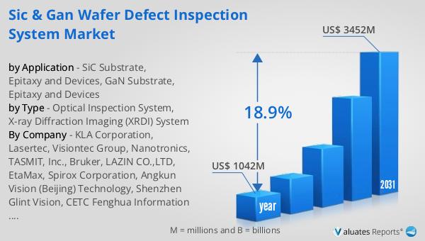
 Figure 10. Global SiC & GaN Wafer Defect Inspection System Production Value (US$ Million), 2020 VS 2024 VS 2031
 Figure 11. Global SiC & GaN Wafer Defect Inspection System Production Value (US$ Million) & (2020-2031)
 Figure 12. Global SiC & GaN Wafer Defect Inspection System Production Capacity (Units) & (2020-2031)
 Figure 13. Global SiC & GaN Wafer Defect Inspection System Production (Units) & (2020-2031)
 Figure 14. Global SiC & GaN Wafer Defect Inspection System Average Price (K US$/Unit) & (2020-2031)
 Figure 15. SiC & GaN Wafer Defect Inspection System Report Years Considered
 Figure 16. SiC & GaN Wafer Defect Inspection System Production Share by Manufacturers in 2024
 Figure 17. Global SiC & GaN Wafer Defect Inspection System Production Value Share by Manufacturers (2024)
 Figure 18. SiC & GaN Wafer Defect Inspection System Market Share by Company Type (Tier 1, Tier 2, and Tier 3): 2020 VS 2024
 Figure 19. The Global 5 and 10 Largest Players: Market Share by SiC & GaN Wafer Defect Inspection System Revenue in 2024
 Figure 20. Global SiC & GaN Wafer Defect Inspection System Production Value by Region: 2020 VS 2024 VS 2031 (US$ Million)
 Figure 21. Global SiC & GaN Wafer Defect Inspection System Production Value Market Share by Region: 2020 VS 2024 VS 2031
 Figure 22. Global SiC & GaN Wafer Defect Inspection System Production Comparison by Region: 2020 VS 2024 VS 2031 (Units)
 Figure 23. Global SiC & GaN Wafer Defect Inspection System Production Market Share by Region: 2020 VS 2024 VS 2031
 Figure 24. North America SiC & GaN Wafer Defect Inspection System Production Value (US$ Million) Growth Rate (2020-2031)
 Figure 25. China SiC & GaN Wafer Defect Inspection System Production Value (US$ Million) Growth Rate (2020-2031)
 Figure 26. Japan SiC & GaN Wafer Defect Inspection System Production Value (US$ Million) Growth Rate (2020-2031)
 Figure 27. South Korea SiC & GaN Wafer Defect Inspection System Production Value (US$ Million) Growth Rate (2020-2031)
 Figure 28. China Taiwan SiC & GaN Wafer Defect Inspection System Production Value (US$ Million) Growth Rate (2020-2031)
 Figure 29. Singapore SiC & GaN Wafer Defect Inspection System Production Value (US$ Million) Growth Rate (2020-2031)
 Figure 30. Global SiC & GaN Wafer Defect Inspection System Consumption by Region: 2020 VS 2024 VS 2031 (Units)
 Figure 31. Global SiC & GaN Wafer Defect Inspection System Consumption Market Share by Region: 2020 VS 2024 VS 2031
 Figure 32. North America SiC & GaN Wafer Defect Inspection System Consumption and Growth Rate (2020-2031) & (Units)
 Figure 33. North America SiC & GaN Wafer Defect Inspection System Consumption Market Share by Country (2020-2031)
 Figure 34. U.S. SiC & GaN Wafer Defect Inspection System Consumption and Growth Rate (2020-2031) & (Units)
 Figure 35. Canada SiC & GaN Wafer Defect Inspection System Consumption and Growth Rate (2020-2031) & (Units)
 Figure 36. Europe SiC & GaN Wafer Defect Inspection System Consumption and Growth Rate (2020-2031) & (Units)
 Figure 37. Europe SiC & GaN Wafer Defect Inspection System Consumption Market Share by Country (2020-2031)
 Figure 38. Germany SiC & GaN Wafer Defect Inspection System Consumption and Growth Rate (2020-2031) & (Units)
 Figure 39. France SiC & GaN Wafer Defect Inspection System Consumption and Growth Rate (2020-2031) & (Units)
 Figure 40. U.K. SiC & GaN Wafer Defect Inspection System Consumption and Growth Rate (2020-2031) & (Units)
 Figure 41. Italy SiC & GaN Wafer Defect Inspection System Consumption and Growth Rate (2020-2031) & (Units)
 Figure 42. Netherlands SiC & GaN Wafer Defect Inspection System Consumption and Growth Rate (2020-2031) & (Units)
 Figure 43. Asia Pacific SiC & GaN Wafer Defect Inspection System Consumption and Growth Rate (2020-2031) & (Units)
 Figure 44. Asia Pacific SiC & GaN Wafer Defect Inspection System Consumption Market Share by Region (2020-2031)
 Figure 45. China SiC & GaN Wafer Defect Inspection System Consumption and Growth Rate (2020-2031) & (Units)
 Figure 46. Japan SiC & GaN Wafer Defect Inspection System Consumption and Growth Rate (2020-2031) & (Units)
 Figure 47. South Korea SiC & GaN Wafer Defect Inspection System Consumption and Growth Rate (2020-2031) & (Units)
 Figure 48. China Taiwan SiC & GaN Wafer Defect Inspection System Consumption and Growth Rate (2020-2031) & (Units)
 Figure 49. Southeast Asia SiC & GaN Wafer Defect Inspection System Consumption and Growth Rate (2020-2031) & (Units)
 Figure 50. India SiC & GaN Wafer Defect Inspection System Consumption and Growth Rate (2020-2031) & (Units)
 Figure 51. Latin America, Middle East & Africa SiC & GaN Wafer Defect Inspection System Consumption and Growth Rate (2020-2031) & (Units)
 Figure 52. Latin America, Middle East & Africa SiC & GaN Wafer Defect Inspection System Consumption Market Share by Country (2020-2031)
 Figure 53. Mexico SiC & GaN Wafer Defect Inspection System Consumption and Growth Rate (2020-2031) & (Units)
 Figure 54. Brazil SiC & GaN Wafer Defect Inspection System Consumption and Growth Rate (2020-2031) & (Units)
 Figure 55. Israel SiC & GaN Wafer Defect Inspection System Consumption and Growth Rate (2020-2031) & (Units)
 Figure 56. Global Production Market Share of SiC & GaN Wafer Defect Inspection System by Type (2020-2031)
 Figure 57. Global Production Value Market Share of SiC & GaN Wafer Defect Inspection System by Type (2020-2031)
 Figure 58. Global SiC & GaN Wafer Defect Inspection System Price (K US$/Unit) by Type (2020-2031)
 Figure 59. Global Production Market Share of SiC & GaN Wafer Defect Inspection System by Application (2020-2031)
 Figure 60. Global Production Value Market Share of SiC & GaN Wafer Defect Inspection System by Application (2020-2031)
 Figure 61. Global SiC & GaN Wafer Defect Inspection System Price (K US$/Unit) by Application (2020-2031)
 Figure 62. SiC & GaN Wafer Defect Inspection System Value Chain
 Figure 63. Channels of Distribution (Direct Vs Distribution)
 Figure 64. Bottom-up and Top-down Approaches for This Report
 Figure 65. Data Triangulation
SELECT A FORMAT
Added to Cart
Electronic (PDF)

$2900

This license allows only one user to access the PDF.
Electronic (PDF)

$4350

This license allows 1 - 5 user to access the PDF, license is suitable for small groups of 5 users working together
Electronic (PDF)

$5800

This license allows users/teams in a same Enterprise to use this report, various departments within an enterpise can use this report
Add to Cart
Buy Now (15% Discount)

OUR CUSTOMER

Strategic Venue Partners

RELATED REPORTS

Global Electric Pressure Calibrator Market Research Report 2025

120 Pages
Type: Report
Code: QYRE-Auto-9J19928
Fri Sep 12 00:00:00 UTC 2025

Add to Cart

Global Semiconductor Defect Inspection Systems Market Research Report 2025

120 Pages
Type: Report
Code: QYRE-Auto-3Q6463
Fri Sep 12 00:00:00 UTC 2025

Add to Cart

Global Low-dielectric Materials for 5G Communication Market Research Report 2025

120 Pages
Type: Report
Code: QYRE-Auto-17U17948
Fri Sep 12 00:00:00 UTC 2025

Add to Cart

Global PC-Based Motion Controller for Semiconductor Market Research Report 2025

120 Pages
Type: Report
Code: QYRE-Auto-22K17724
Fri Sep 12 00:00:00 UTC 2025

Add to Cart