0
U.S. (TOLL FREE)
+1 (315) 215-3225
Automative

0
U.S. (TOLL FREE)
+1 (315) 215-3225
Global Semiconductor Advanced Packaging Lithography System Market Research Report 2026
Published Date: 2026-01-30
|
Report Code: QYRE-Auto-14Z20275
Home | Market Reports | Computers & Electronics| Electronics & Electrical| Electronic Components
Global Semiconductor Advanced Packaging Lithography System Market Research Report 2026
BUY CHAPTERS

Global Semiconductor Advanced Packaging Lithography System Market Research Report 2026

Code: QYRE-Auto-14Z20275
Report
2026-01-30
Pages:127
QYResearch
Buy Now with 15% Discount
DESCRIPTION
TABLE OF CONTENT
TABLES & FIGURES

Semiconductor Advanced Packaging Lithography System Market Size

The global Semiconductor Advanced Packaging Lithography System market was valued at US$ 286 million in 2025 and is anticipated to reach US$ 513 million by 2032, at a CAGR of 8.8% from 2026 to 2032.

Semiconductor Advanced Packaging Lithography System Market

Semiconductor Advanced Packaging Lithography System Market

The 2025 U.S. tariff policies introduce profound uncertainty into the global economic landscape. This report critically examines the implications of recent tariff adjustments and international strategic countermeasures on Semiconductor Advanced Packaging Lithography System competitive dynamics, regional economic interdependencies, and supply chain reconfigurations.
Semiconductor advanced packaging lithography machines are different from front-end chip lithography machines. Advanced packaging lithography machines are key production equipment in the semiconductor packaging process (FOWLP, WLCSP, TSV, etc.). Their main function is to transfer precise circuit patterns to the packaging substrate or chip surface during the chip packaging stage to achieve high-density and high-performance electronic devices. Front-end lithography machines are mainly used in the wafer preparation process. They project the designed chip circuit pattern onto the silicon wafer through the projection method to form a tiny circuit pattern, which plays a vital role in the chip processing process and lays a good foundation for subsequent steps.
The price of semiconductor advanced packaging lithography machines depends on the resolution, wafer size, etc. The resolution of lithography machines of different companies varies to a certain extent. For example, the highest resolution of K&S lithography machine is 1.2μm. Globally, the advanced packaging lithography machine market is mainly concentrated in the hands of several leading companies, such as K&S, Onto, Ushio, Canon, etc., and the top 5 share exceeds 75%.
The North American market for Semiconductor Advanced Packaging Lithography System is projected to increase from US$ million in 2025 to US$ million by 2032, at a CAGR of % over 2026–2032.
The Asia-Pacific market for Semiconductor Advanced Packaging Lithography System is projected to rise from US$ million in 2025 to US$ million by 2032, at a CAGR of % over 2026–2032.
Major global manufacturers of Semiconductor Advanced Packaging Lithography System include Onto Innovation, Ushio, Canon, Kulicke and Soffa Industries, Veeco, Shanghai Micro Electronics Equipment, Circuit Fabology Microelectronics Equipment, etc. In 2025, the world's top three vendors accounted for approximately % of revenue.
This report delivers a comprehensive overview of the global Semiconductor Advanced Packaging Lithography System market, with both quantitative and qualitative analyses, to help readers develop growth strategies, assess the competitive landscape, evaluate their position in the current market, and make informed business decisions regarding Semiconductor Advanced Packaging Lithography System. The Semiconductor Advanced Packaging Lithography System market size, estimates, and forecasts are provided in terms of shipments (Units) and revenue (US$ millions), with 2025 as the base year and historical and forecast data for 2021–2032.
The report segments the global Semiconductor Advanced Packaging Lithography System market comprehensively. Regional market sizes by Type, by Application, , and by company are also provided. For deeper insight, the report profiles the competitive landscape, key competitors, and their respective market rankings, and discusses technological trends and new product developments.
This report will assist Semiconductor Advanced Packaging Lithography System manufacturers, new entrants, and companies across the industry value chain with information on revenues, production, and average prices for the overall market and its sub-segments, by company, by Type, by Application, and by region.
Market Segmentation

Scope of Semiconductor Advanced Packaging Lithography System Market Report

Report Metric Details
Report Name Semiconductor Advanced Packaging Lithography System Market
Accounted market size in 2025 US$ 286 million
Forecasted market size in 2032 US$ 513 million
CAGR 8.8%
Base Year 2025
Forecasted years 2026 - 2032
Segment by Type
  • 200mm Wafer
  • 300mm Wafer
  • Others
by Application
  • Wafer Level Packaging
  • 2.5/3D Packaging
  • FC Packaging
  • Others
Production by Region
  • North America
  • Europe
  • China
  • Japan
  • South Korea
Consumption by Region
  • North America (United States, Canada)
  • Europe (Germany, France, UK, Italy, Russia)
  • Asia-Pacific (China, Japan, South Korea, Taiwan)
  • Southeast Asia (India)
  • Latin America (Mexico, Brazil)
By Company Onto Innovation, Ushio, Canon, Kulicke and Soffa Industries, Veeco, Shanghai Micro Electronics Equipment, Circuit Fabology Microelectronics Equipment
Forecast units USD million in value
Report coverage Revenue and volume forecast, company share, competitive landscape, growth factors and trends

Chapter Outline

  • Chapter 1: Defines the scope of the report and presents an executive summary of market segments (by Type, by Application, , etc.), including the size of each segment and its future growth potential. It offers a high-level view of the current market and its likely evolution in the short, medium, and long term.
  • Chapter 2: Provides a detailed analysis of the competitive landscape for Semiconductor Advanced Packaging Lithography System manufacturers, including prices, production, value-based market shares, latest development plans, and information on mergers and acquisitions.
  • Chapter 3: Examines Semiconductor Advanced Packaging Lithography System production/output and value by region and country, providing a quantitative assessment of market size and growth potential for each region over the next six years.
  • Chapter 4: Analyzes Semiconductor Advanced Packaging Lithography System consumption at the regional and country levels. It quantifies market size and growth potential for each region and its key countries, and outlines market development, outlook, addressable space, and national production.
  • Chapter 5: Analyzes market segments by Type, covering the size and growth potential of each segment to help readers identify “blue ocean” opportunities.
  • Chapter 6: Analyzes market segments by Application, covering the size and growth potential of each segment to help readers identify “blue ocean” opportunities in downstream markets.
  • Chapter 7: Profiles key players, detailing the fundamentals of major companies, including product production/output, value, price, gross margin, product portfolio/introductions, and recent developments.
  • Chapter 8: Reviews the industry value chain, including upstream and downstream segments.
  • Chapter 9: Discusses market dynamics and recent developments, including drivers, restraints, challenges and risks for manufacturers, U.S. Tariffs and relevant policy analysis.
  • Chapter 10: Summarizes the key findings and conclusions of the report.

FAQ for this report

How fast is Semiconductor Advanced Packaging Lithography System Market growing?

Ans: The Semiconductor Advanced Packaging Lithography System Market witnessing a CAGR of 8.8% during the forecast period 2026-2032.

What is the Semiconductor Advanced Packaging Lithography System Market size in 2032?

Ans: The Semiconductor Advanced Packaging Lithography System Market size in 2032 will be US$ 513 million.

What is the market share of major companies in Semiconductor Advanced Packaging Lithography System Market?

Ans: Globally, the advanced packaging lithography machine market is mainly concentrated in the hands of several leading companies, such as K&S, Onto, Ushio, Canon, etc., and the top 5 share exceeds 75%.

Who are the main players in the Semiconductor Advanced Packaging Lithography System Market report?

Ans: The main players in the Semiconductor Advanced Packaging Lithography System Market are Onto Innovation, Ushio, Canon, Kulicke and Soffa Industries, Veeco, Shanghai Micro Electronics Equipment, Circuit Fabology Microelectronics Equipment

What are the Application segmentation covered in the Semiconductor Advanced Packaging Lithography System Market report?

Ans: The Applications covered in the Semiconductor Advanced Packaging Lithography System Market report are Wafer Level Packaging, 2.5/3D Packaging, FC Packaging, Others

What are the Type segmentation covered in the Semiconductor Advanced Packaging Lithography System Market report?

Ans: The Types covered in the Semiconductor Advanced Packaging Lithography System Market report are 200mm Wafer, 300mm Wafer, Others

1 Semiconductor Advanced Packaging Lithography System Market Overview
1.1 Product Definition
1.2 Semiconductor Advanced Packaging Lithography System by Type
1.2.1 Global Semiconductor Advanced Packaging Lithography System Market Value Growth Rate Analysis by Type: 2025 vs 2032
1.2.2 200mm Wafer
1.2.3 300mm Wafer
1.2.4 Others
1.3 Semiconductor Advanced Packaging Lithography System by Application
1.3.1 Global Semiconductor Advanced Packaging Lithography System Market Value Growth Rate Analysis by Application: 2025 vs 2032
1.3.2 Wafer Level Packaging
1.3.3 2.5/3D Packaging
1.3.4 FC Packaging
1.3.5 Others
1.4 Global Market Growth Prospects
1.4.1 Global Semiconductor Advanced Packaging Lithography System Production Value Estimates and Forecasts (2021–2032)
1.4.2 Global Semiconductor Advanced Packaging Lithography System Production Capacity Estimates and Forecasts (2021–2032)
1.4.3 Global Semiconductor Advanced Packaging Lithography System Production Estimates and Forecasts (2021–2032)
1.4.4 Global Semiconductor Advanced Packaging Lithography System Market Average Price Estimates and Forecasts (2021–2032)
1.5 Assumptions and Limitations
2 Market Competition by Manufacturers
2.1 Global Semiconductor Advanced Packaging Lithography System Production Market Share by Manufacturers (2021–2026)
2.2 Global Semiconductor Advanced Packaging Lithography System Production Value Market Share by Manufacturers (2021–2026)
2.3 Global Key Players of Semiconductor Advanced Packaging Lithography System, Industry Ranking, 2024 vs 2025
2.4 Global Semiconductor Advanced Packaging Lithography System Market Share by Company Tier (Tier 1, Tier 2, Tier 3)
2.5 Global Semiconductor Advanced Packaging Lithography System Average Price by Manufacturers (2021–2026)
2.6 Global Key Manufacturers of Semiconductor Advanced Packaging Lithography System, Manufacturing Footprints and Headquarters
2.7 Global Key Manufacturers of Semiconductor Advanced Packaging Lithography System, Product Offerings and Applications
2.8 Global Key Manufacturers of Semiconductor Advanced Packaging Lithography System, Date of Entry into the Industry
2.9 Semiconductor Advanced Packaging Lithography System Market Competitive Situation and Trends
2.9.1 Semiconductor Advanced Packaging Lithography System Market Concentration Rate
2.9.2 Top 5 and Top 10 Global Semiconductor Advanced Packaging Lithography System Players Market Share by Revenue
2.10 Mergers & Acquisitions and Expansion
3 Semiconductor Advanced Packaging Lithography System Production by Region
3.1 Global Semiconductor Advanced Packaging Lithography System Production Value Estimates and Forecasts by Region: 2021 vs 2025 vs 2032
3.2 Global Semiconductor Advanced Packaging Lithography System Production Value by Region (2021–2032)
3.2.1 Global Semiconductor Advanced Packaging Lithography System Production Value by Region (2021–2026)
3.2.2 Global Forecasted Production Value of Semiconductor Advanced Packaging Lithography System by Region (2027–2032)
3.3 Global Semiconductor Advanced Packaging Lithography System Production Estimates and Forecasts by Region: 2021 vs 2025 vs 2032
3.4 Global Semiconductor Advanced Packaging Lithography System Production Volume by Region (2021–2032)
3.4.1 Global Semiconductor Advanced Packaging Lithography System Production by Region (2021–2026)
3.4.2 Global Forecasted Production of Semiconductor Advanced Packaging Lithography System by Region (2027–2032)
3.5 Global Semiconductor Advanced Packaging Lithography System Market Price Analysis by Region (2021–2026)
3.6 Global Semiconductor Advanced Packaging Lithography System Production, Value, and Year-over-Year Growth
3.6.1 North America Semiconductor Advanced Packaging Lithography System Production Value Estimates and Forecasts (2021–2032)
3.6.2 Europe Semiconductor Advanced Packaging Lithography System Production Value Estimates and Forecasts (2021–2032)
3.6.3 China Semiconductor Advanced Packaging Lithography System Production Value Estimates and Forecasts (2021–2032)
3.6.4 Japan Semiconductor Advanced Packaging Lithography System Production Value Estimates and Forecasts (2021–2032)
3.6.5 South Korea Semiconductor Advanced Packaging Lithography System Production Value Estimates and Forecasts (2021–2032)
4 Semiconductor Advanced Packaging Lithography System Consumption by Region
4.1 Global Semiconductor Advanced Packaging Lithography System Consumption Estimates and Forecasts by Region: 2021 vs 2025 vs 2032
4.2 Global Semiconductor Advanced Packaging Lithography System Consumption by Region (2021–2032)
4.2.1 Global Semiconductor Advanced Packaging Lithography System Consumption by Region (2021–2026)
4.2.2 Global Semiconductor Advanced Packaging Lithography System Forecasted Consumption by Region (2027–2032)
4.3 North America
4.3.1 North America Semiconductor Advanced Packaging Lithography System Consumption Growth Rate by Country: 2021 vs 2025 vs 2032
4.3.2 North America Semiconductor Advanced Packaging Lithography System Consumption by Country (2021–2032)
4.3.3 U.S.
4.3.4 Canada
4.4 Europe
4.4.1 Europe Semiconductor Advanced Packaging Lithography System Consumption Growth Rate by Country: 2021 vs 2025 vs 2032
4.4.2 Europe Semiconductor Advanced Packaging Lithography System Consumption by Country (2021–2032)
4.4.3 Germany
4.4.4 France
4.4.5 U.K.
4.4.6 Italy
4.4.7 Russia
4.5 Asia Pacific
4.5.1 Asia Pacific Semiconductor Advanced Packaging Lithography System Consumption Growth Rate by Region: 2021 vs 2025 vs 2032
4.5.2 Asia Pacific Semiconductor Advanced Packaging Lithography System Consumption by Region (2021–2032)
4.5.3 China
4.5.4 Japan
4.5.5 South Korea
4.5.6 China Taiwan
4.5.7 Southeast Asia
4.5.8 India
4.6 Latin America, Middle East & Africa
4.6.1 Latin America, Middle East & Africa Semiconductor Advanced Packaging Lithography System Consumption Growth Rate by Country: 2021 vs 2025 vs 2032
4.6.2 Latin America, Middle East & Africa Semiconductor Advanced Packaging Lithography System Consumption by Country (2021–2032)
4.6.3 Mexico
4.6.4 Brazil
4.6.5 Israel
4.6.6 GCC Countries
5 Segment by Type
5.1 Global Semiconductor Advanced Packaging Lithography System Production by Type (2021–2032)
5.1.1 Global Semiconductor Advanced Packaging Lithography System Production by Type (2021–2026)
5.1.2 Global Semiconductor Advanced Packaging Lithography System Production by Type (2027–2032)
5.1.3 Global Semiconductor Advanced Packaging Lithography System Production Market Share by Type (2021–2032)
5.2 Global Semiconductor Advanced Packaging Lithography System Production Value by Type (2021–2032)
5.2.1 Global Semiconductor Advanced Packaging Lithography System Production Value by Type (2021–2026)
5.2.2 Global Semiconductor Advanced Packaging Lithography System Production Value by Type (2027–2032)
5.2.3 Global Semiconductor Advanced Packaging Lithography System Production Value Market Share by Type (2021–2032)
5.3 Global Semiconductor Advanced Packaging Lithography System Price by Type (2021–2032)
6 Segment by Application
6.1 Global Semiconductor Advanced Packaging Lithography System Production by Application (2021–2032)
6.1.1 Global Semiconductor Advanced Packaging Lithography System Production by Application (2021–2026)
6.1.2 Global Semiconductor Advanced Packaging Lithography System Production by Application (2027–2032)
6.1.3 Global Semiconductor Advanced Packaging Lithography System Production Market Share by Application (2021–2032)
6.2 Global Semiconductor Advanced Packaging Lithography System Production Value by Application (2021–2032)
6.2.1 Global Semiconductor Advanced Packaging Lithography System Production Value by Application (2021–2026)
6.2.2 Global Semiconductor Advanced Packaging Lithography System Production Value by Application (2027–2032)
6.2.3 Global Semiconductor Advanced Packaging Lithography System Production Value Market Share by Application (2021–2032)
6.3 Global Semiconductor Advanced Packaging Lithography System Price by Application (2021–2032)
7 Key Companies Profiled
7.1 Onto Innovation
7.1.1 Onto Innovation Semiconductor Advanced Packaging Lithography System Company Information
7.1.2 Onto Innovation Semiconductor Advanced Packaging Lithography System Product Portfolio
7.1.3 Onto Innovation Semiconductor Advanced Packaging Lithography System Production, Value, Price, and Gross Margin (2021–2026)
7.1.4 Onto Innovation Main Business and Markets Served
7.1.5 Onto Innovation Recent Developments/Updates
7.2 Ushio
7.2.1 Ushio Semiconductor Advanced Packaging Lithography System Company Information
7.2.2 Ushio Semiconductor Advanced Packaging Lithography System Product Portfolio
7.2.3 Ushio Semiconductor Advanced Packaging Lithography System Production, Value, Price, and Gross Margin (2021–2026)
7.2.4 Ushio Main Business and Markets Served
7.2.5 Ushio Recent Developments/Updates
7.3 Canon
7.3.1 Canon Semiconductor Advanced Packaging Lithography System Company Information
7.3.2 Canon Semiconductor Advanced Packaging Lithography System Product Portfolio
7.3.3 Canon Semiconductor Advanced Packaging Lithography System Production, Value, Price, and Gross Margin (2021–2026)
7.3.4 Canon Main Business and Markets Served
7.3.5 Canon Recent Developments/Updates
7.4 Kulicke and Soffa Industries
7.4.1 Kulicke and Soffa Industries Semiconductor Advanced Packaging Lithography System Company Information
7.4.2 Kulicke and Soffa Industries Semiconductor Advanced Packaging Lithography System Product Portfolio
7.4.3 Kulicke and Soffa Industries Semiconductor Advanced Packaging Lithography System Production, Value, Price, and Gross Margin (2021–2026)
7.4.4 Kulicke and Soffa Industries Main Business and Markets Served
7.4.5 Kulicke and Soffa Industries Recent Developments/Updates
7.5 Veeco
7.5.1 Veeco Semiconductor Advanced Packaging Lithography System Company Information
7.5.2 Veeco Semiconductor Advanced Packaging Lithography System Product Portfolio
7.5.3 Veeco Semiconductor Advanced Packaging Lithography System Production, Value, Price, and Gross Margin (2021–2026)
7.5.4 Veeco Main Business and Markets Served
7.5.5 Veeco Recent Developments/Updates
7.6 Shanghai Micro Electronics Equipment
7.6.1 Shanghai Micro Electronics Equipment Semiconductor Advanced Packaging Lithography System Company Information
7.6.2 Shanghai Micro Electronics Equipment Semiconductor Advanced Packaging Lithography System Product Portfolio
7.6.3 Shanghai Micro Electronics Equipment Semiconductor Advanced Packaging Lithography System Production, Value, Price, and Gross Margin (2021–2026)
7.6.4 Shanghai Micro Electronics Equipment Main Business and Markets Served
7.6.5 Shanghai Micro Electronics Equipment Recent Developments/Updates
7.7 Circuit Fabology Microelectronics Equipment
7.7.1 Circuit Fabology Microelectronics Equipment Semiconductor Advanced Packaging Lithography System Company Information
7.7.2 Circuit Fabology Microelectronics Equipment Semiconductor Advanced Packaging Lithography System Product Portfolio
7.7.3 Circuit Fabology Microelectronics Equipment Semiconductor Advanced Packaging Lithography System Production, Value, Price, and Gross Margin (2021–2026)
7.7.4 Circuit Fabology Microelectronics Equipment Main Business and Markets Served
7.7.5 Circuit Fabology Microelectronics Equipment Recent Developments/Updates
8 Industry Chain and Sales Channels Analysis
8.1 Semiconductor Advanced Packaging Lithography System Industry Chain Analysis
8.2 Semiconductor Advanced Packaging Lithography System Raw Material Supply Analysis
8.2.1 Key Raw Materials
8.2.2 Raw Materials Key Suppliers
8.3 Semiconductor Advanced Packaging Lithography System Production Modes and Processes
8.4 Semiconductor Advanced Packaging Lithography System Sales and Marketing
8.4.1 Semiconductor Advanced Packaging Lithography System Sales Channels
8.4.2 Semiconductor Advanced Packaging Lithography System Distributors
8.5 Semiconductor Advanced Packaging Lithography System Customer Analysis
9 Semiconductor Advanced Packaging Lithography System Market Dynamics
9.1 Semiconductor Advanced Packaging Lithography System Industry Trends
9.2 Semiconductor Advanced Packaging Lithography System Market Drivers
9.3 Semiconductor Advanced Packaging Lithography System Market Challenges
9.4 Semiconductor Advanced Packaging Lithography System Market Restraints
9.5 Impact of U.S. Tariffs
10 Research Findings and Conclusion
11 Methodology and Data Source
11.1 Methodology/Research Approach
11.1.1 Research Programs/Design
11.1.2 Market Size Estimation
11.1.3 Market Breakdown and Data Triangulation
11.2 Data Source
11.2.1 Secondary Sources
11.2.2 Primary Sources
11.3 Author List
11.4 Disclaimer
List of Tables
 Table 1. Global Semiconductor Advanced Packaging Lithography System Market Value by Type (US$ Million), 2025 vs 2032
 Table 2. Global Semiconductor Advanced Packaging Lithography System Market Value by Application (US$ Million), 2025 vs 2032
 Table 3. Global Semiconductor Advanced Packaging Lithography System Production Capacity (Units) by Manufacturers in 2025
 Table 4. Global Semiconductor Advanced Packaging Lithography System Production by Manufacturers (Units), 2021–2026
 Table 5. Global Semiconductor Advanced Packaging Lithography System Production Market Share by Manufacturers (2021–2026)
 Table 6. Global Semiconductor Advanced Packaging Lithography System Production Value by Manufacturers (US$ Million), 2021–2026
 Table 7. Global Semiconductor Advanced Packaging Lithography System Production Value Share by Manufacturers (2021–2026)
 Table 8. Global Key Players of Semiconductor Advanced Packaging Lithography System, Industry Ranking, 2024 vs 2025
 Table 9. Classification of Companies by Tier (Tier 1, Tier 2, Tier 3), based on Semiconductor Advanced Packaging Lithography System Production Value, 2025
 Table 10. Global Market Semiconductor Advanced Packaging Lithography System Average Price by Manufacturers (K US$/Unit), 2021–2026
 Table 11. Global Key Manufacturers of Semiconductor Advanced Packaging Lithography System, Manufacturing Footprints and Headquarters
 Table 12. Global Key Manufacturers of Semiconductor Advanced Packaging Lithography System, Product Offerings and Applications
 Table 13. Global Key Manufacturers of Semiconductor Advanced Packaging Lithography System, Date of Entry into the Industry
 Table 14. Global Semiconductor Advanced Packaging Lithography System Manufacturers Market Concentration Ratio (CR5 and HHI)
 Table 15. Mergers & Acquisitions and Expansion Plans
 Table 16. Global Semiconductor Advanced Packaging Lithography System Production Value by Region: 2021 vs 2025 vs 2032 (US$ Million)
 Table 17. Global Semiconductor Advanced Packaging Lithography System Production Value (US$ Million) by Region (2021–2026)
 Table 18. Global Semiconductor Advanced Packaging Lithography System Production Value Market Share by Region (2021–2026)
 Table 19. Global Semiconductor Advanced Packaging Lithography System Production Value (US$ Million) Forecast by Region (2027–2032)
 Table 20. Global Semiconductor Advanced Packaging Lithography System Production Value Market Share Forecast by Region (2027–2032)
 Table 21. Global Semiconductor Advanced Packaging Lithography System Production Comparison by Region: 2021 vs 2025 vs 2032 (Units)
 Table 22. Global Semiconductor Advanced Packaging Lithography System Production (Units) by Region (2021–2026)
 Table 23. Global Semiconductor Advanced Packaging Lithography System Production Market Share by Region (2021–2026)
 Table 24. Global Semiconductor Advanced Packaging Lithography System Production (Units) Forecast by Region (2027–2032)
 Table 25. Global Semiconductor Advanced Packaging Lithography System Production Market Share Forecast by Region (2027–2032)
 Table 26. Global Semiconductor Advanced Packaging Lithography System Market Average Price (K US$/Unit) by Region (2021–2026)
 Table 27. Global Semiconductor Advanced Packaging Lithography System Market Average Price (K US$/Unit) by Region (2027–2032)
 Table 28. Global Semiconductor Advanced Packaging Lithography System Consumption Growth Rate by Region: 2021 vs 2025 vs 2032 (Units)
 Table 29. Global Semiconductor Advanced Packaging Lithography System Consumption by Region (Units), 2021–2026
 Table 30. Global Semiconductor Advanced Packaging Lithography System Consumption Market Share by Region (2021–2026)
 Table 31. Global Semiconductor Advanced Packaging Lithography System Forecasted Consumption by Region (Units), 2027–2032
 Table 32. Global Semiconductor Advanced Packaging Lithography System Forecasted Consumption Market Share by Region (2027–2032)
 Table 33. North America Semiconductor Advanced Packaging Lithography System Consumption Growth Rate by Country: 2021 vs 2025 vs 2032 (Units)
 Table 34. North America Semiconductor Advanced Packaging Lithography System Consumption by Country (Units), 2021–2026
 Table 35. North America Semiconductor Advanced Packaging Lithography System Consumption by Country (Units), 2027–2032
 Table 36. Europe Semiconductor Advanced Packaging Lithography System Consumption Growth Rate by Country: 2021 vs 2025 vs 2032 (Units)
 Table 37. Europe Semiconductor Advanced Packaging Lithography System Consumption by Country (Units), 2021–2026
 Table 38. Europe Semiconductor Advanced Packaging Lithography System Consumption by Country (Units), 2027–2032
 Table 39. Asia Pacific Semiconductor Advanced Packaging Lithography System Consumption Growth Rate by Region: 2021 vs 2025 vs 2032 (Units)
 Table 40. Asia Pacific Semiconductor Advanced Packaging Lithography System Consumption by Region (Units), 2021–2026
 Table 41. Asia Pacific Semiconductor Advanced Packaging Lithography System Consumption by Region (Units), 2027–2032
 Table 42. Latin America, Middle East & Africa Semiconductor Advanced Packaging Lithography System Consumption Growth Rate by Country: 2021 vs 2025 vs 2032 (Units)
 Table 43. Latin America, Middle East & Africa Semiconductor Advanced Packaging Lithography System Consumption by Country (Units), 2021–2026
 Table 44. Latin America, Middle East & Africa Semiconductor Advanced Packaging Lithography System Consumption by Country (Units), 2027–2032
 Table 45. Global Semiconductor Advanced Packaging Lithography System Production (Units) by Type (2021–2026)
 Table 46. Global Semiconductor Advanced Packaging Lithography System Production (Units) by Type (2027–2032)
 Table 47. Global Semiconductor Advanced Packaging Lithography System Production Market Share by Type (2021–2026)
 Table 48. Global Semiconductor Advanced Packaging Lithography System Production Market Share by Type (2027–2032)
 Table 49. Global Semiconductor Advanced Packaging Lithography System Production Value (US$ Million) by Type (2021–2026)
 Table 50. Global Semiconductor Advanced Packaging Lithography System Production Value (US$ Million) by Type (2027–2032)
 Table 51. Global Semiconductor Advanced Packaging Lithography System Production Value Market Share by Type (2021–2026)
 Table 52. Global Semiconductor Advanced Packaging Lithography System Production Value Market Share by Type (2027–2032)
 Table 53. Global Semiconductor Advanced Packaging Lithography System Price (K US$/Unit) by Type (2021–2026)
 Table 54. Global Semiconductor Advanced Packaging Lithography System Price (K US$/Unit) by Type (2027–2032)
 Table 55. Global Semiconductor Advanced Packaging Lithography System Production (Units) by Application (2021–2026)
 Table 56. Global Semiconductor Advanced Packaging Lithography System Production (Units) by Application (2027–2032)
 Table 57. Global Semiconductor Advanced Packaging Lithography System Production Market Share by Application (2021–2026)
 Table 58. Global Semiconductor Advanced Packaging Lithography System Production Market Share by Application (2027–2032)
 Table 59. Global Semiconductor Advanced Packaging Lithography System Production Value (US$ Million) by Application (2021–2026)
 Table 60. Global Semiconductor Advanced Packaging Lithography System Production Value (US$ Million) by Application (2027–2032)
 Table 61. Global Semiconductor Advanced Packaging Lithography System Production Value Market Share by Application (2021–2026)
 Table 62. Global Semiconductor Advanced Packaging Lithography System Production Value Market Share by Application (2027–2032)
 Table 63. Global Semiconductor Advanced Packaging Lithography System Price (K US$/Unit) by Application (2021–2026)
 Table 64. Global Semiconductor Advanced Packaging Lithography System Price (K US$/Unit) by Application (2027–2032)
 Table 65. Onto Innovation Semiconductor Advanced Packaging Lithography System Company Information
 Table 66. Onto Innovation Semiconductor Advanced Packaging Lithography System Specification and Application
 Table 67. Onto Innovation Semiconductor Advanced Packaging Lithography System Production (Units), Value (US$ Million), Price (K US$/Unit) and Gross Margin (2021–2026)
 Table 68. Onto Innovation Main Business and Markets Served
 Table 69. Onto Innovation Recent Developments/Updates
 Table 70. Ushio Semiconductor Advanced Packaging Lithography System Company Information
 Table 71. Ushio Semiconductor Advanced Packaging Lithography System Specification and Application
 Table 72. Ushio Semiconductor Advanced Packaging Lithography System Production (Units), Value (US$ Million), Price (K US$/Unit) and Gross Margin (2021–2026)
 Table 73. Ushio Main Business and Markets Served
 Table 74. Ushio Recent Developments/Updates
 Table 75. Canon Semiconductor Advanced Packaging Lithography System Company Information
 Table 76. Canon Semiconductor Advanced Packaging Lithography System Specification and Application
 Table 77. Canon Semiconductor Advanced Packaging Lithography System Production (Units), Value (US$ Million), Price (K US$/Unit) and Gross Margin (2021–2026)
 Table 78. Canon Main Business and Markets Served
 Table 79. Canon Recent Developments/Updates
 Table 80. Kulicke and Soffa Industries Semiconductor Advanced Packaging Lithography System Company Information
 Table 81. Kulicke and Soffa Industries Semiconductor Advanced Packaging Lithography System Specification and Application
 Table 82. Kulicke and Soffa Industries Semiconductor Advanced Packaging Lithography System Production (Units), Value (US$ Million), Price (K US$/Unit) and Gross Margin (2021–2026)
 Table 83. Kulicke and Soffa Industries Main Business and Markets Served
 Table 84. Kulicke and Soffa Industries Recent Developments/Updates
 Table 85. Veeco Semiconductor Advanced Packaging Lithography System Company Information
 Table 86. Veeco Semiconductor Advanced Packaging Lithography System Specification and Application
 Table 87. Veeco Semiconductor Advanced Packaging Lithography System Production (Units), Value (US$ Million), Price (K US$/Unit) and Gross Margin (2021–2026)
 Table 88. Veeco Main Business and Markets Served
 Table 89. Veeco Recent Developments/Updates
 Table 90. Shanghai Micro Electronics Equipment Semiconductor Advanced Packaging Lithography System Company Information
 Table 91. Shanghai Micro Electronics Equipment Semiconductor Advanced Packaging Lithography System Specification and Application
 Table 92. Shanghai Micro Electronics Equipment Semiconductor Advanced Packaging Lithography System Production (Units), Value (US$ Million), Price (K US$/Unit) and Gross Margin (2021–2026)
 Table 93. Shanghai Micro Electronics Equipment Main Business and Markets Served
 Table 94. Shanghai Micro Electronics Equipment Recent Developments/Updates
 Table 95. Circuit Fabology Microelectronics Equipment Semiconductor Advanced Packaging Lithography System Company Information
 Table 96. Circuit Fabology Microelectronics Equipment Semiconductor Advanced Packaging Lithography System Specification and Application
 Table 97. Circuit Fabology Microelectronics Equipment Semiconductor Advanced Packaging Lithography System Production (Units), Value (US$ Million), Price (K US$/Unit) and Gross Margin (2021–2026)
 Table 98. Circuit Fabology Microelectronics Equipment Main Business and Markets Served
 Table 99. Circuit Fabology Microelectronics Equipment Recent Developments/Updates
 Table 100. Key Raw Materials Lists
 Table 101. Raw Materials Key Suppliers Lists
 Table 102. Semiconductor Advanced Packaging Lithography System Distributors List
 Table 103. Semiconductor Advanced Packaging Lithography System Customers List
 Table 104. Semiconductor Advanced Packaging Lithography System Market Trends
 Table 105. Semiconductor Advanced Packaging Lithography System Market Drivers
 Table 106. Semiconductor Advanced Packaging Lithography System Market Challenges
 Table 107. Semiconductor Advanced Packaging Lithography System Market Restraints
 Table 108. Research Programs/Design for This Report
 Table 109. Key Data Information from Secondary Sources
 Table 110. Key Data Information from Primary Sources
 Table 111. Authors List of This Report


List of Figures
 Figure 1. Product Picture of Semiconductor Advanced Packaging Lithography System
 Figure 2. Global Semiconductor Advanced Packaging Lithography System Market Value by Type (US$ Million), 2021–2032
 Figure 3. Global Semiconductor Advanced Packaging Lithography System Market Share by Type: 2025 vs 2032
 Figure 4. 200mm Wafer Product Picture
 Figure 5. 300mm Wafer Product Picture
 Figure 6. Others Product Picture
 Figure 7. Global Semiconductor Advanced Packaging Lithography System Market Value by Application (US$ Million), 2021–2032
 Figure 8. Global Semiconductor Advanced Packaging Lithography System Market Share by Application: 2025 vs 2032
 Figure 9. Wafer Level Packaging
 Figure 10. 2.5/3D Packaging
 Figure 11. FC Packaging
 Figure 12. Others
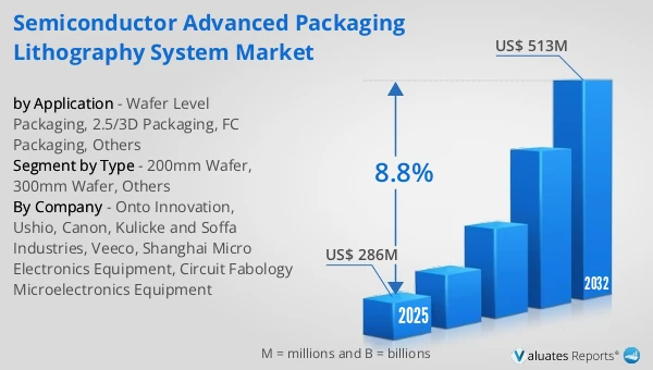
 Figure 13. Global Semiconductor Advanced Packaging Lithography System Production Value (US$ Million), 2021 vs 2025 vs 2032
 Figure 14. Global Semiconductor Advanced Packaging Lithography System Production Value (US$ Million), 2021–2032
 Figure 15. Global Semiconductor Advanced Packaging Lithography System Production Capacity (Units), 2021–2032
 Figure 16. Global Semiconductor Advanced Packaging Lithography System Production (Units), 2021–2032
 Figure 17. Global Semiconductor Advanced Packaging Lithography System Average Price (K US$/Unit), 2021–2032
 Figure 18. Semiconductor Advanced Packaging Lithography System Report Years Considered
 Figure 19. Semiconductor Advanced Packaging Lithography System Production Share by Manufacturers in 2025
 Figure 20. Global Semiconductor Advanced Packaging Lithography System Production Value Share by Manufacturers (2025)
 Figure 21. Semiconductor Advanced Packaging Lithography System Market Share by Company Type (Tier 1, Tier 2, and Tier 3): 2021 vs 2025
 Figure 22. Top 5 and Top 10 Global Players: Market Share by Semiconductor Advanced Packaging Lithography System Revenue in 2025
 Figure 23. Global Semiconductor Advanced Packaging Lithography System Production Value by Region: 2021 vs 2025 vs 2032 (US$ Million)
 Figure 24. Global Semiconductor Advanced Packaging Lithography System Production Value Market Share by Region: 2021 vs 2025 vs 2032
 Figure 25. Global Semiconductor Advanced Packaging Lithography System Production Comparison by Region: 2021 vs 2025 vs 2032 (Units)
 Figure 26. Global Semiconductor Advanced Packaging Lithography System Production Market Share by Region: 2021 vs 2025 vs 2032
 Figure 27. North America Semiconductor Advanced Packaging Lithography System Production Value (US$ Million) Growth Rate (2021–2032)
 Figure 28. Europe Semiconductor Advanced Packaging Lithography System Production Value (US$ Million) Growth Rate (2021–2032)
 Figure 29. China Semiconductor Advanced Packaging Lithography System Production Value (US$ Million) Growth Rate (2021–2032)
 Figure 30. Japan Semiconductor Advanced Packaging Lithography System Production Value (US$ Million) Growth Rate (2021–2032)
 Figure 31. South Korea Semiconductor Advanced Packaging Lithography System Production Value (US$ Million) Growth Rate (2021–2032)
 Figure 32. Global Semiconductor Advanced Packaging Lithography System Consumption by Region: 2021 vs 2025 vs 2032 (Units)
 Figure 33. Global Semiconductor Advanced Packaging Lithography System Consumption Market Share by Region: 2021 vs 2025 vs 2032
 Figure 34. North America Semiconductor Advanced Packaging Lithography System Consumption and Growth Rate (Units), 2021–2032
 Figure 35. North America Semiconductor Advanced Packaging Lithography System Consumption Market Share by Country (2021–2032)
 Figure 36. U.S. Semiconductor Advanced Packaging Lithography System Consumption and Growth Rate (Units), 2021–2032
 Figure 37. Canada Semiconductor Advanced Packaging Lithography System Consumption and Growth Rate (Units), 2021–2032
 Figure 38. Europe Semiconductor Advanced Packaging Lithography System Consumption and Growth Rate (Units), 2021–2032
 Figure 39. Europe Semiconductor Advanced Packaging Lithography System Consumption Market Share by Country (2021–2032)
 Figure 40. Germany Semiconductor Advanced Packaging Lithography System Consumption and Growth Rate (Units), 2021–2032
 Figure 41. France Semiconductor Advanced Packaging Lithography System Consumption and Growth Rate (Units), 2021–2032
 Figure 42. U.K. Semiconductor Advanced Packaging Lithography System Consumption and Growth Rate (Units), 2021–2032
 Figure 43. Italy Semiconductor Advanced Packaging Lithography System Consumption and Growth Rate (Units), 2021–2032
 Figure 44. Russia Semiconductor Advanced Packaging Lithography System Consumption and Growth Rate (Units), 2021–2032
 Figure 45. Asia Pacific Semiconductor Advanced Packaging Lithography System Consumption and Growth Rate (Units), 2021–2032
 Figure 46. Asia Pacific Semiconductor Advanced Packaging Lithography System Consumption Market Share by Region (2021–2032)
 Figure 47. China Semiconductor Advanced Packaging Lithography System Consumption and Growth Rate (Units), 2021–2032
 Figure 48. Japan Semiconductor Advanced Packaging Lithography System Consumption and Growth Rate (Units), 2021–2032
 Figure 49. South Korea Semiconductor Advanced Packaging Lithography System Consumption and Growth Rate (Units), 2021–2032
 Figure 50. China Taiwan Semiconductor Advanced Packaging Lithography System Consumption and Growth Rate (Units), 2021–2032
 Figure 51. Southeast Asia Semiconductor Advanced Packaging Lithography System Consumption and Growth Rate (Units), 2021–2032
 Figure 52. India Semiconductor Advanced Packaging Lithography System Consumption and Growth Rate (Units), 2021–2032
 Figure 53. Latin America, Middle East & Africa Semiconductor Advanced Packaging Lithography System Consumption and Growth Rate (Units), 2021–2032
 Figure 54. Latin America, Middle East & Africa Semiconductor Advanced Packaging Lithography System Consumption Market Share by Country (2021–2032)
 Figure 55. Mexico Semiconductor Advanced Packaging Lithography System Consumption and Growth Rate (Units), 2021–2032
 Figure 56. Brazil Semiconductor Advanced Packaging Lithography System Consumption and Growth Rate (Units), 2021–2032
 Figure 57. Israel Semiconductor Advanced Packaging Lithography System Consumption and Growth Rate (Units), 2021–2032
 Figure 58. GCC Countries Semiconductor Advanced Packaging Lithography System Consumption and Growth Rate (Units), 2021–2032
 Figure 59. Global Production Market Share of Semiconductor Advanced Packaging Lithography System by Type (2021–2032)
 Figure 60. Global Production Value Market Share of Semiconductor Advanced Packaging Lithography System by Type (2021–2032)
 Figure 61. Global Semiconductor Advanced Packaging Lithography System Price (K US$/Unit) by Type (2021–2032)
 Figure 62. Global Production Market Share of Semiconductor Advanced Packaging Lithography System by Application (2021–2032)
 Figure 63. Global Production Value Market Share of Semiconductor Advanced Packaging Lithography System by Application (2021–2032)
 Figure 64. Global Semiconductor Advanced Packaging Lithography System Price (K US$/Unit) by Application (2021–2032)
 Figure 65. Semiconductor Advanced Packaging Lithography System Value Chain
 Figure 66. Channels of Distribution (Direct Vs Distribution)
 Figure 67. Bottom-up and Top-down Approaches for This Report
 Figure 68. Data Triangulation
SELECT A FORMAT
Added to Cart
Electronic

$2900

Single User License
Electronic

$4350

Multi User License
Electronic

$5800

Enterprise License
Add to Cart
Buy Now (15% Discount)

OUR CUSTOMER

Nano Dimension

SIMILAR REPORTS