0
U.S. (TOLL FREE)
+1 (315) 215-3225
Automative

0
U.S. (TOLL FREE)
+1 (315) 215-3225
Global Semiconductor Grade PEEK Profiles Market Research Report 2026
Published Date: 2026-01-19
|
Report Code: QYRE-Auto-15X18889
Home | Market Reports
Global Semiconductor Grade PEEK Profiles Market Research Report 2024
BUY CHAPTERS

Global Semiconductor Grade PEEK Profiles Market Research Report 2026

Code: QYRE-Auto-15X18889
Report
2026-01-19
Pages:136
QYResearch
Buy Now with 15% Discount
DESCRIPTION
TABLE OF CONTENT
TABLES & FIGURES

Semiconductor Grade PEEK Profiles Market Size

The global Semiconductor Grade PEEK Profiles market was valued at US$ 366 million in 2025 and is anticipated to reach US$ 591 million by 2032, at a CAGR of 7.2% from 2026 to 2032.

Semiconductor Grade PEEK Profiles Market

Semiconductor Grade PEEK Profiles Market

The 2025 U.S. tariff policies introduce profound uncertainty into the global economic landscape. This report critically examines the implications of recent tariff adjustments and international strategic countermeasures on Semiconductor Grade PEEK Profiles competitive dynamics, regional economic interdependencies, and supply chain reconfigurations.
In 2024, global Semiconductor Grade PEEK Profiles production reached approximately 4.21 K tons, with an average global market price of around 80.2 USD/kg.
Semiconductor Grade PEEK Profiles are high-purity, customized-shaped functional components made from polyetheretherketone (PEEK) resin, processed into forms such as plates, rods, and tubes through precision extrusion or molding. They feature ultra-high purity, low volatility, and minimal particle generation, combined with PEEK’s inherent advantages of high temperature resistance (long-term service at 260°C), excellent chemical corrosion resistance, stable electrical insulation, and good dimensional stability. Strictly controlled for impurities and static properties, they avoid contaminating wafers or causing electrostatic damage, making them ideal for manufacturing semiconductor process components like CMP retainer rings, wafer carriers, and chip clamping parts, which play a key role in improving production efficiency and wafer yield.
The single-line production capacity of Semiconductor Grade PEEK Profiles is 228 to 235 tons per year, the average gross profit margin was 42.8%.
The cost structure of Semiconductor Grade PEEK Profiles is dominated by four core components with clear weights: raw material costs account for the largest share at 50%-60%, mainly including high-purity PEEK resin, anti-static modifiers, and functional additives. The high price of high-purity PEEK resin and the cost of specialized modifiers directly drive up the overall cost. Production and processing costs make up 25%-30%, covering precision extrusion/molding, high-temperature annealing, precision cutting, and strict cleanliness testing. Strict control over dimensional accuracy, surface smoothness, and particle content to meet semiconductor process requirements increases manufacturing complexity. R&D costs represent 10%-15%, dedicated to optimizing purification technology (reducing impurity content), developing anti-static and low-outgassing variants, and adapting to the processing needs of advanced semiconductor processes, as high technological barriers are core to market competition. Packaging and logistics costs constitute the remaining 4%-6%, including cleanroom-grade sealed packaging (to prevent contamination) and dust-free transportation, with storage requiring clean and dry conditions to maintain product purity.
The industry chain of Semiconductor Grade PEEK Profiles consists of three interconnected tiers: upstream includes suppliers of chemical raw materials (fluoroketone, hydroquinone, diphenyl sulfone), high-purity PEEK resin, functional additives, production equipment (precision extruders, cleanroom processing tools), and testing instruments (particle detectors, chemical resistance testers). Midstream involves enterprises engaged in resin modification, precision molding, profile processing, and quality calibration, focusing on adjusting product purity, static resistance, and dimensional specifications to meet the strict requirements of semiconductor manufacturing processes. Downstream covers semiconductor wafer fabs, semiconductor equipment manufacturers, and advanced packaging and testing enterprises, with demand driven by the upgrading of semiconductor process nodes, the expansion of third-generation semiconductor production, and the replacement of traditional metal and engineering plastic components.
Demand for Semiconductor Grade PEEK Profiles is growing rapidly driven by the global advancement of semiconductor process nodes, the increasing demand for high-purity and corrosion-resistant process components, and the expansion of third-generation semiconductor industries. It addresses pain points such as easy contamination and poor durability of traditional materials in semiconductor manufacturing, while the low domestic substitution rate in high-end segments provides broad market space. Key business opportunities lie in developing high-precision profiles for advanced process CMP equipment, optimizing anti-static and low-outgassing performance to adapt to extreme process environments, and expanding applications in third-generation semiconductor material processing. Additionally, strengthening independent R&D of high-purity PEEK resin to reduce reliance on imports and collaborating with semiconductor equipment manufacturers for customized solutions can further tap into the high-growth potential of the semiconductor functional component market.
This report delivers a comprehensive overview of the global Semiconductor Grade PEEK Profiles market, with both quantitative and qualitative analyses, to help readers develop growth strategies, assess the competitive landscape, evaluate their position in the current market, and make informed business decisions regarding Semiconductor Grade PEEK Profiles. The Semiconductor Grade PEEK Profiles market size, estimates, and forecasts are provided in terms of shipments (Tons) and revenue (US$ millions), with 2025 as the base year and historical and forecast data for 2021–2032.
The report segments the global Semiconductor Grade PEEK Profiles market comprehensively. Regional market sizes by Profile Form, by Application, by Purity, and by company are also provided. For deeper insight, the report profiles the competitive landscape, key competitors, and their respective market rankings, and discusses technological trends and new product developments.
This report will assist Semiconductor Grade PEEK Profiles manufacturers, new entrants, and companies across the industry value chain with information on revenues, production, and average prices for the overall market and its sub-segments, by company, by Profile Form, by Application, and by region.
Market Segmentation

Scope of Semiconductor Grade PEEK Profiles Market Report

Report Metric Details
Report Name Semiconductor Grade PEEK Profiles Market
Accounted market size in 2025 US$ 366 million
Forecasted market size in 2032 US$ 591 million
CAGR 7.2%
Base Year 2025
Forecasted years 2026 - 2032
Segment by Profile Form
  • Rod Profiles
  • Plate and Sheet Profiles
  • Tube and Pipe Profiles
  • Custom Extruded Profiles
Segment by Purity
  • Standard Cleanroom Grade
  • High Purity Grade
  • Ultra High Purity Grade
  • Metal-Ion Controlled Grade
Segment by Reinforcement Type
  • Unfilled PEEK Profiles
  • Glass-Fiber Reinforced Profiles
  • Carbon-Fiber Reinforced Profiles
  • Lubricant-Filled Wear-Resistant Profiles
by Application
  • Wafer Handling and Carrier Components
  • Etch and Deposition Tool Parts
  • CMP and Wet-Process Module Components
  • Test Socket and Probe Hardware
Production by Region
  • North America
  • Europe
  • China
  • Japan
Consumption by Region
  • North America (United States, Canada)
  • Europe (Germany, France, UK, Italy, Russia)
  • Asia-Pacific (China, Japan, South Korea, Taiwan)
  • Southeast Asia (India)
  • Latin America (Mexico, Brazil)
By Company Ensinger, Röchling Industrial, Dongguan Noegem Plastic products, Junhua PEEK, Shenzhen WOTE Advanced Materials, Eweiger, Zero Engineering, Suzhou Jutai HPM, PBI Advanced Materials, Mitsubishi Chemical, Polymore Materials, Nanjing Shousu, Zhejiang Conceptfe New Material Technology, Victrex, RTP Company
Forecast units USD million in value
Report coverage Revenue and volume forecast, company share, competitive landscape, growth factors and trends

Chapter Outline

  • Chapter 1: Defines the scope of the report and presents an executive summary of market segments (by Profile Form, by Application, by Purity, etc.), including the size of each segment and its future growth potential. It offers a high-level view of the current market and its likely evolution in the short, medium, and long term.
  • Chapter 2: Provides a detailed analysis of the competitive landscape for Semiconductor Grade PEEK Profiles manufacturers, including prices, production, value-based market shares, latest development plans, and information on mergers and acquisitions.
  • Chapter 3: Examines Semiconductor Grade PEEK Profiles production/output and value by region and country, providing a quantitative assessment of market size and growth potential for each region over the next six years.
  • Chapter 4: Analyzes Semiconductor Grade PEEK Profiles consumption at the regional and country levels. It quantifies market size and growth potential for each region and its key countries, and outlines market development, outlook, addressable space, and national production.
  • Chapter 5: Analyzes market segments by Profile Form, covering the size and growth potential of each segment to help readers identify “blue ocean” opportunities.
  • Chapter 6: Analyzes market segments by Application, covering the size and growth potential of each segment to help readers identify “blue ocean” opportunities in downstream markets.
  • Chapter 7: Profiles key players, detailing the fundamentals of major companies, including product production/output, value, price, gross margin, product portfolio/introductions, and recent developments.
  • Chapter 8: Reviews the industry value chain, including upstream and downstream segments.
  • Chapter 9: Discusses market dynamics and recent developments, including drivers, restraints, challenges and risks for manufacturers, U.S. Tariffs and relevant policy analysis.
  • Chapter 10: Summarizes the key findings and conclusions of the report.

FAQ for this report

How fast is Semiconductor Grade PEEK Profiles Market growing?

Ans: The Semiconductor Grade PEEK Profiles Market witnessing a CAGR of 7.2% during the forecast period 2026-2032.

What is the Semiconductor Grade PEEK Profiles Market size in 2032?

Ans: The Semiconductor Grade PEEK Profiles Market size in 2032 will be US$ 591 million.

Who are the main players in the Semiconductor Grade PEEK Profiles Market report?

Ans: The main players in the Semiconductor Grade PEEK Profiles Market are Ensinger, Röchling Industrial, Dongguan Noegem Plastic products, Junhua PEEK, Shenzhen WOTE Advanced Materials, Eweiger, Zero Engineering, Suzhou Jutai HPM, PBI Advanced Materials, Mitsubishi Chemical, Polymore Materials, Nanjing Shousu, Zhejiang Conceptfe New Material Technology, Victrex, RTP Company

What are the Application segmentation covered in the Semiconductor Grade PEEK Profiles Market report?

Ans: The Applications covered in the Semiconductor Grade PEEK Profiles Market report are Wafer Handling and Carrier Components, Etch and Deposition Tool Parts, CMP and Wet-Process Module Components, Test Socket and Probe Hardware

What are the Type segmentation covered in the Semiconductor Grade PEEK Profiles Market report?

Ans: The Types covered in the Semiconductor Grade PEEK Profiles Market report are Unfilled PEEK Profiles, Glass-Fiber Reinforced Profiles, Carbon-Fiber Reinforced Profiles, Lubricant-Filled Wear-Resistant Profiles

1 Semiconductor Grade PEEK Profiles Market Overview
1.1 Product Definition
1.2 Semiconductor Grade PEEK Profiles by Profile Form
1.2.1 Global Semiconductor Grade PEEK Profiles Market Value Growth Rate Analysis by Profile Form: 2025 vs 2032
1.2.2 Rod Profiles
1.2.3 Plate and Sheet Profiles
1.2.4 Tube and Pipe Profiles
1.2.5 Custom Extruded Profiles
1.3 Semiconductor Grade PEEK Profiles by Purity
1.3.1 Global Semiconductor Grade PEEK Profiles Market Value Growth Rate Analysis by Purity: 2025 vs 2032
1.3.2 Standard Cleanroom Grade
1.3.3 High Purity Grade
1.3.4 Ultra High Purity Grade
1.3.5 Metal-Ion Controlled Grade
1.4 Semiconductor Grade PEEK Profiles by Reinforcement Type
1.4.1 Global Semiconductor Grade PEEK Profiles Market Value Growth Rate Analysis by Reinforcement Type: 2025 vs 2032
1.4.2 Unfilled PEEK Profiles
1.4.3 Glass-Fiber Reinforced Profiles
1.4.4 Carbon-Fiber Reinforced Profiles
1.4.5 Lubricant-Filled Wear-Resistant Profiles
1.5 Semiconductor Grade PEEK Profiles by Application
1.5.1 Global Semiconductor Grade PEEK Profiles Market Value Growth Rate Analysis by Application: 2025 vs 2032
1.5.2 Wafer Handling and Carrier Components
1.5.3 Etch and Deposition Tool Parts
1.5.4 CMP and Wet-Process Module Components
1.5.5 Test Socket and Probe Hardware
1.6 Global Market Growth Prospects
1.6.1 Global Semiconductor Grade PEEK Profiles Production Value Estimates and Forecasts (2021–2032)
1.6.2 Global Semiconductor Grade PEEK Profiles Production Capacity Estimates and Forecasts (2021–2032)
1.6.3 Global Semiconductor Grade PEEK Profiles Production Estimates and Forecasts (2021–2032)
1.6.4 Global Semiconductor Grade PEEK Profiles Market Average Price Estimates and Forecasts (2021–2032)
1.7 Assumptions and Limitations
2 Market Competition by Manufacturers
2.1 Global Semiconductor Grade PEEK Profiles Production Market Share by Manufacturers (2021–2026)
2.2 Global Semiconductor Grade PEEK Profiles Production Value Market Share by Manufacturers (2021–2026)
2.3 Global Key Players of Semiconductor Grade PEEK Profiles, Industry Ranking, 2024 vs 2025
2.4 Global Semiconductor Grade PEEK Profiles Market Share by Company Tier (Tier 1, Tier 2, Tier 3)
2.5 Global Semiconductor Grade PEEK Profiles Average Price by Manufacturers (2021–2026)
2.6 Global Key Manufacturers of Semiconductor Grade PEEK Profiles, Manufacturing Footprints and Headquarters
2.7 Global Key Manufacturers of Semiconductor Grade PEEK Profiles, Product Offerings and Applications
2.8 Global Key Manufacturers of Semiconductor Grade PEEK Profiles, Date of Entry into the Industry
2.9 Semiconductor Grade PEEK Profiles Market Competitive Situation and Trends
2.9.1 Semiconductor Grade PEEK Profiles Market Concentration Rate
2.9.2 Top 5 and Top 10 Global Semiconductor Grade PEEK Profiles Players Market Share by Revenue
2.10 Mergers & Acquisitions and Expansion
3 Semiconductor Grade PEEK Profiles Production by Region
3.1 Global Semiconductor Grade PEEK Profiles Production Value Estimates and Forecasts by Region: 2021 vs 2025 vs 2032
3.2 Global Semiconductor Grade PEEK Profiles Production Value by Region (2021–2032)
3.2.1 Global Semiconductor Grade PEEK Profiles Production Value by Region (2021–2026)
3.2.2 Global Forecasted Production Value of Semiconductor Grade PEEK Profiles by Region (2027–2032)
3.3 Global Semiconductor Grade PEEK Profiles Production Estimates and Forecasts by Region: 2021 vs 2025 vs 2032
3.4 Global Semiconductor Grade PEEK Profiles Production Volume by Region (2021–2032)
3.4.1 Global Semiconductor Grade PEEK Profiles Production by Region (2021–2026)
3.4.2 Global Forecasted Production of Semiconductor Grade PEEK Profiles by Region (2027–2032)
3.5 Global Semiconductor Grade PEEK Profiles Market Price Analysis by Region (2021–2026)
3.6 Global Semiconductor Grade PEEK Profiles Production, Value, and Year-over-Year Growth
3.6.1 North America Semiconductor Grade PEEK Profiles Production Value Estimates and Forecasts (2021–2032)
3.6.2 Europe Semiconductor Grade PEEK Profiles Production Value Estimates and Forecasts (2021–2032)
3.6.3 China Semiconductor Grade PEEK Profiles Production Value Estimates and Forecasts (2021–2032)
3.6.4 Japan Semiconductor Grade PEEK Profiles Production Value Estimates and Forecasts (2021–2032)
4 Semiconductor Grade PEEK Profiles Consumption by Region
4.1 Global Semiconductor Grade PEEK Profiles Consumption Estimates and Forecasts by Region: 2021 vs 2025 vs 2032
4.2 Global Semiconductor Grade PEEK Profiles Consumption by Region (2021–2032)
4.2.1 Global Semiconductor Grade PEEK Profiles Consumption by Region (2021–2026)
4.2.2 Global Semiconductor Grade PEEK Profiles Forecasted Consumption by Region (2027–2032)
4.3 North America
4.3.1 North America Semiconductor Grade PEEK Profiles Consumption Growth Rate by Country: 2021 vs 2025 vs 2032
4.3.2 North America Semiconductor Grade PEEK Profiles Consumption by Country (2021–2032)
4.3.3 U.S.
4.3.4 Canada
4.4 Europe
4.4.1 Europe Semiconductor Grade PEEK Profiles Consumption Growth Rate by Country: 2021 vs 2025 vs 2032
4.4.2 Europe Semiconductor Grade PEEK Profiles Consumption by Country (2021–2032)
4.4.3 Germany
4.4.4 France
4.4.5 U.K.
4.4.6 Italy
4.4.7 Russia
4.5 Asia Pacific
4.5.1 Asia Pacific Semiconductor Grade PEEK Profiles Consumption Growth Rate by Region: 2021 vs 2025 vs 2032
4.5.2 Asia Pacific Semiconductor Grade PEEK Profiles Consumption by Region (2021–2032)
4.5.3 China
4.5.4 Japan
4.5.5 South Korea
4.5.6 China Taiwan
4.5.7 Southeast Asia
4.5.8 India
4.6 Latin America, Middle East & Africa
4.6.1 Latin America, Middle East & Africa Semiconductor Grade PEEK Profiles Consumption Growth Rate by Country: 2021 vs 2025 vs 2032
4.6.2 Latin America, Middle East & Africa Semiconductor Grade PEEK Profiles Consumption by Country (2021–2032)
4.6.3 Mexico
4.6.4 Brazil
4.6.5 Turkey
4.6.6 GCC Countries
5 Segment by Profile Form
5.1 Global Semiconductor Grade PEEK Profiles Production by Profile Form (2021–2032)
5.1.1 Global Semiconductor Grade PEEK Profiles Production by Profile Form (2021–2026)
5.1.2 Global Semiconductor Grade PEEK Profiles Production by Profile Form (2027–2032)
5.1.3 Global Semiconductor Grade PEEK Profiles Production Market Share by Profile Form (2021–2032)
5.2 Global Semiconductor Grade PEEK Profiles Production Value by Profile Form (2021–2032)
5.2.1 Global Semiconductor Grade PEEK Profiles Production Value by Profile Form (2021–2026)
5.2.2 Global Semiconductor Grade PEEK Profiles Production Value by Profile Form (2027–2032)
5.2.3 Global Semiconductor Grade PEEK Profiles Production Value Market Share by Profile Form (2021–2032)
5.3 Global Semiconductor Grade PEEK Profiles Price by Profile Form (2021–2032)
6 Segment by Application
6.1 Global Semiconductor Grade PEEK Profiles Production by Application (2021–2032)
6.1.1 Global Semiconductor Grade PEEK Profiles Production by Application (2021–2026)
6.1.2 Global Semiconductor Grade PEEK Profiles Production by Application (2027–2032)
6.1.3 Global Semiconductor Grade PEEK Profiles Production Market Share by Application (2021–2032)
6.2 Global Semiconductor Grade PEEK Profiles Production Value by Application (2021–2032)
6.2.1 Global Semiconductor Grade PEEK Profiles Production Value by Application (2021–2026)
6.2.2 Global Semiconductor Grade PEEK Profiles Production Value by Application (2027–2032)
6.2.3 Global Semiconductor Grade PEEK Profiles Production Value Market Share by Application (2021–2032)
6.3 Global Semiconductor Grade PEEK Profiles Price by Application (2021–2032)
7 Key Companies Profiled
7.1 Ensinger
7.1.1 Ensinger Semiconductor Grade PEEK Profiles Company Information
7.1.2 Ensinger Semiconductor Grade PEEK Profiles Product Portfolio
7.1.3 Ensinger Semiconductor Grade PEEK Profiles Production, Value, Price, and Gross Margin (2021–2026)
7.1.4 Ensinger Main Business and Markets Served
7.1.5 Ensinger Recent Developments/Updates
7.2 Röchling Industrial
7.2.1 Röchling Industrial Semiconductor Grade PEEK Profiles Company Information
7.2.2 Röchling Industrial Semiconductor Grade PEEK Profiles Product Portfolio
7.2.3 Röchling Industrial Semiconductor Grade PEEK Profiles Production, Value, Price, and Gross Margin (2021–2026)
7.2.4 Röchling Industrial Main Business and Markets Served
7.2.5 Röchling Industrial Recent Developments/Updates
7.3 Dongguan Noegem Plastic products
7.3.1 Dongguan Noegem Plastic products Semiconductor Grade PEEK Profiles Company Information
7.3.2 Dongguan Noegem Plastic products Semiconductor Grade PEEK Profiles Product Portfolio
7.3.3 Dongguan Noegem Plastic products Semiconductor Grade PEEK Profiles Production, Value, Price, and Gross Margin (2021–2026)
7.3.4 Dongguan Noegem Plastic products Main Business and Markets Served
7.3.5 Dongguan Noegem Plastic products Recent Developments/Updates
7.4 Junhua PEEK
7.4.1 Junhua PEEK Semiconductor Grade PEEK Profiles Company Information
7.4.2 Junhua PEEK Semiconductor Grade PEEK Profiles Product Portfolio
7.4.3 Junhua PEEK Semiconductor Grade PEEK Profiles Production, Value, Price, and Gross Margin (2021–2026)
7.4.4 Junhua PEEK Main Business and Markets Served
7.4.5 Junhua PEEK Recent Developments/Updates
7.5 Shenzhen WOTE Advanced Materials
7.5.1 Shenzhen WOTE Advanced Materials Semiconductor Grade PEEK Profiles Company Information
7.5.2 Shenzhen WOTE Advanced Materials Semiconductor Grade PEEK Profiles Product Portfolio
7.5.3 Shenzhen WOTE Advanced Materials Semiconductor Grade PEEK Profiles Production, Value, Price, and Gross Margin (2021–2026)
7.5.4 Shenzhen WOTE Advanced Materials Main Business and Markets Served
7.5.5 Shenzhen WOTE Advanced Materials Recent Developments/Updates
7.6 Eweiger
7.6.1 Eweiger Semiconductor Grade PEEK Profiles Company Information
7.6.2 Eweiger Semiconductor Grade PEEK Profiles Product Portfolio
7.6.3 Eweiger Semiconductor Grade PEEK Profiles Production, Value, Price, and Gross Margin (2021–2026)
7.6.4 Eweiger Main Business and Markets Served
7.6.5 Eweiger Recent Developments/Updates
7.7 Zero Engineering
7.7.1 Zero Engineering Semiconductor Grade PEEK Profiles Company Information
7.7.2 Zero Engineering Semiconductor Grade PEEK Profiles Product Portfolio
7.7.3 Zero Engineering Semiconductor Grade PEEK Profiles Production, Value, Price, and Gross Margin (2021–2026)
7.7.4 Zero Engineering Main Business and Markets Served
7.7.5 Zero Engineering Recent Developments/Updates
7.8 Suzhou Jutai HPM
7.8.1 Suzhou Jutai HPM Semiconductor Grade PEEK Profiles Company Information
7.8.2 Suzhou Jutai HPM Semiconductor Grade PEEK Profiles Product Portfolio
7.8.3 Suzhou Jutai HPM Semiconductor Grade PEEK Profiles Production, Value, Price, and Gross Margin (2021–2026)
7.8.4 Suzhou Jutai HPM Main Business and Markets Served
7.8.5 Suzhou Jutai HPM Recent Developments/Updates
7.9 PBI Advanced Materials
7.9.1 PBI Advanced Materials Semiconductor Grade PEEK Profiles Company Information
7.9.2 PBI Advanced Materials Semiconductor Grade PEEK Profiles Product Portfolio
7.9.3 PBI Advanced Materials Semiconductor Grade PEEK Profiles Production, Value, Price, and Gross Margin (2021–2026)
7.9.4 PBI Advanced Materials Main Business and Markets Served
7.9.5 PBI Advanced Materials Recent Developments/Updates
7.10 Mitsubishi Chemical
7.10.1 Mitsubishi Chemical Semiconductor Grade PEEK Profiles Company Information
7.10.2 Mitsubishi Chemical Semiconductor Grade PEEK Profiles Product Portfolio
7.10.3 Mitsubishi Chemical Semiconductor Grade PEEK Profiles Production, Value, Price, and Gross Margin (2021–2026)
7.10.4 Mitsubishi Chemical Main Business and Markets Served
7.10.5 Mitsubishi Chemical Recent Developments/Updates
7.11 Polymore Materials
7.11.1 Polymore Materials Semiconductor Grade PEEK Profiles Company Information
7.11.2 Polymore Materials Semiconductor Grade PEEK Profiles Product Portfolio
7.11.3 Polymore Materials Semiconductor Grade PEEK Profiles Production, Value, Price, and Gross Margin (2021–2026)
7.11.4 Polymore Materials Main Business and Markets Served
7.11.5 Polymore Materials Recent Developments/Updates
7.12 Nanjing Shousu
7.12.1 Nanjing Shousu Semiconductor Grade PEEK Profiles Company Information
7.12.2 Nanjing Shousu Semiconductor Grade PEEK Profiles Product Portfolio
7.12.3 Nanjing Shousu Semiconductor Grade PEEK Profiles Production, Value, Price, and Gross Margin (2021–2026)
7.12.4 Nanjing Shousu Main Business and Markets Served
7.12.5 Nanjing Shousu Recent Developments/Updates
7.13 Zhejiang Conceptfe New Material Technology
7.13.1 Zhejiang Conceptfe New Material Technology Semiconductor Grade PEEK Profiles Company Information
7.13.2 Zhejiang Conceptfe New Material Technology Semiconductor Grade PEEK Profiles Product Portfolio
7.13.3 Zhejiang Conceptfe New Material Technology Semiconductor Grade PEEK Profiles Production, Value, Price, and Gross Margin (2021–2026)
7.13.4 Zhejiang Conceptfe New Material Technology Main Business and Markets Served
7.13.5 Zhejiang Conceptfe New Material Technology Recent Developments/Updates
7.14 Victrex
7.14.1 Victrex Semiconductor Grade PEEK Profiles Company Information
7.14.2 Victrex Semiconductor Grade PEEK Profiles Product Portfolio
7.14.3 Victrex Semiconductor Grade PEEK Profiles Production, Value, Price, and Gross Margin (2021–2026)
7.14.4 Victrex Main Business and Markets Served
7.14.5 Victrex Recent Developments/Updates
7.15 RTP Company
7.15.1 RTP Company Semiconductor Grade PEEK Profiles Company Information
7.15.2 RTP Company Semiconductor Grade PEEK Profiles Product Portfolio
7.15.3 RTP Company Semiconductor Grade PEEK Profiles Production, Value, Price, and Gross Margin (2021–2026)
7.15.4 RTP Company Main Business and Markets Served
7.15.5 RTP Company Recent Developments/Updates
8 Industry Chain and Sales Channels Analysis
8.1 Semiconductor Grade PEEK Profiles Industry Chain Analysis
8.2 Semiconductor Grade PEEK Profiles Raw Material Supply Analysis
8.2.1 Key Raw Materials
8.2.2 Raw Materials Key Suppliers
8.3 Semiconductor Grade PEEK Profiles Production Modes and Processes
8.4 Semiconductor Grade PEEK Profiles Sales and Marketing
8.4.1 Semiconductor Grade PEEK Profiles Sales Channels
8.4.2 Semiconductor Grade PEEK Profiles Distributors
8.5 Semiconductor Grade PEEK Profiles Customer Analysis
9 Semiconductor Grade PEEK Profiles Market Dynamics
9.1 Semiconductor Grade PEEK Profiles Industry Trends
9.2 Semiconductor Grade PEEK Profiles Market Drivers
9.3 Semiconductor Grade PEEK Profiles Market Challenges
9.4 Semiconductor Grade PEEK Profiles Market Restraints
9.5 Impact of U.S. Tariffs
10 Research Findings and Conclusion
11 Methodology and Data Source
11.1 Methodology/Research Approach
11.1.1 Research Programs/Design
11.1.2 Market Size Estimation
11.1.3 Market Breakdown and Data Triangulation
11.2 Data Source
11.2.1 Secondary Sources
11.2.2 Primary Sources
11.3 Author List
11.4 Disclaimer
List of Tables
 Table 1. Global Semiconductor Grade PEEK Profiles Market Value by Profile Form (US$ Million), 2025 vs 2032
 Table 2. Global Semiconductor Grade PEEK Profiles Market Value by Purity (US$ Million), 2025 vs 2032
 Table 3. Global Semiconductor Grade PEEK Profiles Market Value by Reinforcement Type (US$ Million), 2025 vs 2032
 Table 4. Global Semiconductor Grade PEEK Profiles Market Value by Application (US$ Million), 2025 vs 2032
 Table 5. Global Semiconductor Grade PEEK Profiles Production Capacity (Tons) by Manufacturers in 2025
 Table 6. Global Semiconductor Grade PEEK Profiles Production by Manufacturers (Tons), 2021–2026
 Table 7. Global Semiconductor Grade PEEK Profiles Production Market Share by Manufacturers (2021–2026)
 Table 8. Global Semiconductor Grade PEEK Profiles Production Value by Manufacturers (US$ Million), 2021–2026
 Table 9. Global Semiconductor Grade PEEK Profiles Production Value Share by Manufacturers (2021–2026)
 Table 10. Global Key Players of Semiconductor Grade PEEK Profiles, Industry Ranking, 2024 vs 2025
 Table 11. Classification of Companies by Tier (Tier 1, Tier 2, Tier 3), based on Semiconductor Grade PEEK Profiles Production Value, 2025
 Table 12. Global Market Semiconductor Grade PEEK Profiles Average Price by Manufacturers (US$/kg), 2021–2026
 Table 13. Global Key Manufacturers of Semiconductor Grade PEEK Profiles, Manufacturing Footprints and Headquarters
 Table 14. Global Key Manufacturers of Semiconductor Grade PEEK Profiles, Product Offerings and Applications
 Table 15. Global Key Manufacturers of Semiconductor Grade PEEK Profiles, Date of Entry into the Industry
 Table 16. Global Semiconductor Grade PEEK Profiles Manufacturers Market Concentration Ratio (CR5 and HHI)
 Table 17. Mergers & Acquisitions and Expansion Plans
 Table 18. Global Semiconductor Grade PEEK Profiles Production Value by Region: 2021 vs 2025 vs 2032 (US$ Million)
 Table 19. Global Semiconductor Grade PEEK Profiles Production Value (US$ Million) by Region (2021–2026)
 Table 20. Global Semiconductor Grade PEEK Profiles Production Value Market Share by Region (2021–2026)
 Table 21. Global Semiconductor Grade PEEK Profiles Production Value (US$ Million) Forecast by Region (2027–2032)
 Table 22. Global Semiconductor Grade PEEK Profiles Production Value Market Share Forecast by Region (2027–2032)
 Table 23. Global Semiconductor Grade PEEK Profiles Production Comparison by Region: 2021 vs 2025 vs 2032 (Tons)
 Table 24. Global Semiconductor Grade PEEK Profiles Production (Tons) by Region (2021–2026)
 Table 25. Global Semiconductor Grade PEEK Profiles Production Market Share by Region (2021–2026)
 Table 26. Global Semiconductor Grade PEEK Profiles Production (Tons) Forecast by Region (2027–2032)
 Table 27. Global Semiconductor Grade PEEK Profiles Production Market Share Forecast by Region (2027–2032)
 Table 28. Global Semiconductor Grade PEEK Profiles Market Average Price (US$/kg) by Region (2021–2026)
 Table 29. Global Semiconductor Grade PEEK Profiles Market Average Price (US$/kg) by Region (2027–2032)
 Table 30. Global Semiconductor Grade PEEK Profiles Consumption Growth Rate by Region: 2021 vs 2025 vs 2032 (Tons)
 Table 31. Global Semiconductor Grade PEEK Profiles Consumption by Region (Tons), 2021–2026
 Table 32. Global Semiconductor Grade PEEK Profiles Consumption Market Share by Region (2021–2026)
 Table 33. Global Semiconductor Grade PEEK Profiles Forecasted Consumption by Region (Tons), 2027–2032
 Table 34. Global Semiconductor Grade PEEK Profiles Forecasted Consumption Market Share by Region (2027–2032)
 Table 35. North America Semiconductor Grade PEEK Profiles Consumption Growth Rate by Country: 2021 vs 2025 vs 2032 (Tons)
 Table 36. North America Semiconductor Grade PEEK Profiles Consumption by Country (Tons), 2021–2026
 Table 37. North America Semiconductor Grade PEEK Profiles Consumption by Country (Tons), 2027–2032
 Table 38. Europe Semiconductor Grade PEEK Profiles Consumption Growth Rate by Country: 2021 vs 2025 vs 2032 (Tons)
 Table 39. Europe Semiconductor Grade PEEK Profiles Consumption by Country (Tons), 2021–2026
 Table 40. Europe Semiconductor Grade PEEK Profiles Consumption by Country (Tons), 2027–2032
 Table 41. Asia Pacific Semiconductor Grade PEEK Profiles Consumption Growth Rate by Region: 2021 vs 2025 vs 2032 (Tons)
 Table 42. Asia Pacific Semiconductor Grade PEEK Profiles Consumption by Region (Tons), 2021–2026
 Table 43. Asia Pacific Semiconductor Grade PEEK Profiles Consumption by Region (Tons), 2027–2032
 Table 44. Latin America, Middle East & Africa Semiconductor Grade PEEK Profiles Consumption Growth Rate by Country: 2021 vs 2025 vs 2032 (Tons)
 Table 45. Latin America, Middle East & Africa Semiconductor Grade PEEK Profiles Consumption by Country (Tons), 2021–2026
 Table 46. Latin America, Middle East & Africa Semiconductor Grade PEEK Profiles Consumption by Country (Tons), 2027–2032
 Table 47. Global Semiconductor Grade PEEK Profiles Production (Tons) by Profile Form (2021–2026)
 Table 48. Global Semiconductor Grade PEEK Profiles Production (Tons) by Profile Form (2027–2032)
 Table 49. Global Semiconductor Grade PEEK Profiles Production Market Share by Profile Form (2021–2026)
 Table 50. Global Semiconductor Grade PEEK Profiles Production Market Share by Profile Form (2027–2032)
 Table 51. Global Semiconductor Grade PEEK Profiles Production Value (US$ Million) by Profile Form (2021–2026)
 Table 52. Global Semiconductor Grade PEEK Profiles Production Value (US$ Million) by Profile Form (2027–2032)
 Table 53. Global Semiconductor Grade PEEK Profiles Production Value Market Share by Profile Form (2021–2026)
 Table 54. Global Semiconductor Grade PEEK Profiles Production Value Market Share by Profile Form (2027–2032)
 Table 55. Global Semiconductor Grade PEEK Profiles Price (US$/kg) by Profile Form (2021–2026)
 Table 56. Global Semiconductor Grade PEEK Profiles Price (US$/kg) by Profile Form (2027–2032)
 Table 57. Global Semiconductor Grade PEEK Profiles Production (Tons) by Application (2021–2026)
 Table 58. Global Semiconductor Grade PEEK Profiles Production (Tons) by Application (2027–2032)
 Table 59. Global Semiconductor Grade PEEK Profiles Production Market Share by Application (2021–2026)
 Table 60. Global Semiconductor Grade PEEK Profiles Production Market Share by Application (2027–2032)
 Table 61. Global Semiconductor Grade PEEK Profiles Production Value (US$ Million) by Application (2021–2026)
 Table 62. Global Semiconductor Grade PEEK Profiles Production Value (US$ Million) by Application (2027–2032)
 Table 63. Global Semiconductor Grade PEEK Profiles Production Value Market Share by Application (2021–2026)
 Table 64. Global Semiconductor Grade PEEK Profiles Production Value Market Share by Application (2027–2032)
 Table 65. Global Semiconductor Grade PEEK Profiles Price (US$/kg) by Application (2021–2026)
 Table 66. Global Semiconductor Grade PEEK Profiles Price (US$/kg) by Application (2027–2032)
 Table 67. Ensinger Semiconductor Grade PEEK Profiles Company Information
 Table 68. Ensinger Semiconductor Grade PEEK Profiles Specification and Application
 Table 69. Ensinger Semiconductor Grade PEEK Profiles Production (Tons), Value (US$ Million), Price (US$/kg) and Gross Margin (2021–2026)
 Table 70. Ensinger Main Business and Markets Served
 Table 71. Ensinger Recent Developments/Updates
 Table 72. Röchling Industrial Semiconductor Grade PEEK Profiles Company Information
 Table 73. Röchling Industrial Semiconductor Grade PEEK Profiles Specification and Application
 Table 74. Röchling Industrial Semiconductor Grade PEEK Profiles Production (Tons), Value (US$ Million), Price (US$/kg) and Gross Margin (2021–2026)
 Table 75. Röchling Industrial Main Business and Markets Served
 Table 76. Röchling Industrial Recent Developments/Updates
 Table 77. Dongguan Noegem Plastic products Semiconductor Grade PEEK Profiles Company Information
 Table 78. Dongguan Noegem Plastic products Semiconductor Grade PEEK Profiles Specification and Application
 Table 79. Dongguan Noegem Plastic products Semiconductor Grade PEEK Profiles Production (Tons), Value (US$ Million), Price (US$/kg) and Gross Margin (2021–2026)
 Table 80. Dongguan Noegem Plastic products Main Business and Markets Served
 Table 81. Dongguan Noegem Plastic products Recent Developments/Updates
 Table 82. Junhua PEEK Semiconductor Grade PEEK Profiles Company Information
 Table 83. Junhua PEEK Semiconductor Grade PEEK Profiles Specification and Application
 Table 84. Junhua PEEK Semiconductor Grade PEEK Profiles Production (Tons), Value (US$ Million), Price (US$/kg) and Gross Margin (2021–2026)
 Table 85. Junhua PEEK Main Business and Markets Served
 Table 86. Junhua PEEK Recent Developments/Updates
 Table 87. Shenzhen WOTE Advanced Materials Semiconductor Grade PEEK Profiles Company Information
 Table 88. Shenzhen WOTE Advanced Materials Semiconductor Grade PEEK Profiles Specification and Application
 Table 89. Shenzhen WOTE Advanced Materials Semiconductor Grade PEEK Profiles Production (Tons), Value (US$ Million), Price (US$/kg) and Gross Margin (2021–2026)
 Table 90. Shenzhen WOTE Advanced Materials Main Business and Markets Served
 Table 91. Shenzhen WOTE Advanced Materials Recent Developments/Updates
 Table 92. Eweiger Semiconductor Grade PEEK Profiles Company Information
 Table 93. Eweiger Semiconductor Grade PEEK Profiles Specification and Application
 Table 94. Eweiger Semiconductor Grade PEEK Profiles Production (Tons), Value (US$ Million), Price (US$/kg) and Gross Margin (2021–2026)
 Table 95. Eweiger Main Business and Markets Served
 Table 96. Eweiger Recent Developments/Updates
 Table 97. Zero Engineering Semiconductor Grade PEEK Profiles Company Information
 Table 98. Zero Engineering Semiconductor Grade PEEK Profiles Specification and Application
 Table 99. Zero Engineering Semiconductor Grade PEEK Profiles Production (Tons), Value (US$ Million), Price (US$/kg) and Gross Margin (2021–2026)
 Table 100. Zero Engineering Main Business and Markets Served
 Table 101. Zero Engineering Recent Developments/Updates
 Table 102. Suzhou Jutai HPM Semiconductor Grade PEEK Profiles Company Information
 Table 103. Suzhou Jutai HPM Semiconductor Grade PEEK Profiles Specification and Application
 Table 104. Suzhou Jutai HPM Semiconductor Grade PEEK Profiles Production (Tons), Value (US$ Million), Price (US$/kg) and Gross Margin (2021–2026)
 Table 105. Suzhou Jutai HPM Main Business and Markets Served
 Table 106. Suzhou Jutai HPM Recent Developments/Updates
 Table 107. PBI Advanced Materials Semiconductor Grade PEEK Profiles Company Information
 Table 108. PBI Advanced Materials Semiconductor Grade PEEK Profiles Specification and Application
 Table 109. PBI Advanced Materials Semiconductor Grade PEEK Profiles Production (Tons), Value (US$ Million), Price (US$/kg) and Gross Margin (2021–2026)
 Table 110. PBI Advanced Materials Main Business and Markets Served
 Table 111. PBI Advanced Materials Recent Developments/Updates
 Table 112. Mitsubishi Chemical Semiconductor Grade PEEK Profiles Company Information
 Table 113. Mitsubishi Chemical Semiconductor Grade PEEK Profiles Specification and Application
 Table 114. Mitsubishi Chemical Semiconductor Grade PEEK Profiles Production (Tons), Value (US$ Million), Price (US$/kg) and Gross Margin (2021–2026)
 Table 115. Mitsubishi Chemical Main Business and Markets Served
 Table 116. Mitsubishi Chemical Recent Developments/Updates
 Table 117. Polymore Materials Semiconductor Grade PEEK Profiles Company Information
 Table 118. Polymore Materials Semiconductor Grade PEEK Profiles Specification and Application
 Table 119. Polymore Materials Semiconductor Grade PEEK Profiles Production (Tons), Value (US$ Million), Price (US$/kg) and Gross Margin (2021–2026)
 Table 120. Polymore Materials Main Business and Markets Served
 Table 121. Polymore Materials Recent Developments/Updates
 Table 122. Nanjing Shousu Semiconductor Grade PEEK Profiles Company Information
 Table 123. Nanjing Shousu Semiconductor Grade PEEK Profiles Specification and Application
 Table 124. Nanjing Shousu Semiconductor Grade PEEK Profiles Production (Tons), Value (US$ Million), Price (US$/kg) and Gross Margin (2021–2026)
 Table 125. Nanjing Shousu Main Business and Markets Served
 Table 126. Nanjing Shousu Recent Developments/Updates
 Table 127. Zhejiang Conceptfe New Material Technology Semiconductor Grade PEEK Profiles Company Information
 Table 128. Zhejiang Conceptfe New Material Technology Semiconductor Grade PEEK Profiles Specification and Application
 Table 129. Zhejiang Conceptfe New Material Technology Semiconductor Grade PEEK Profiles Production (Tons), Value (US$ Million), Price (US$/kg) and Gross Margin (2021–2026)
 Table 130. Zhejiang Conceptfe New Material Technology Main Business and Markets Served
 Table 131. Zhejiang Conceptfe New Material Technology Recent Developments/Updates
 Table 132. Victrex Semiconductor Grade PEEK Profiles Company Information
 Table 133. Victrex Semiconductor Grade PEEK Profiles Specification and Application
 Table 134. Victrex Semiconductor Grade PEEK Profiles Production (Tons), Value (US$ Million), Price (US$/kg) and Gross Margin (2021–2026)
 Table 135. Victrex Main Business and Markets Served
 Table 136. Victrex Recent Developments/Updates
 Table 137. RTP Company Semiconductor Grade PEEK Profiles Company Information
 Table 138. RTP Company Semiconductor Grade PEEK Profiles Specification and Application
 Table 139. RTP Company Semiconductor Grade PEEK Profiles Production (Tons), Value (US$ Million), Price (US$/kg) and Gross Margin (2021–2026)
 Table 140. RTP Company Main Business and Markets Served
 Table 141. RTP Company Recent Developments/Updates
 Table 142. Key Raw Materials Lists
 Table 143. Raw Materials Key Suppliers Lists
 Table 144. Semiconductor Grade PEEK Profiles Distributors List
 Table 145. Semiconductor Grade PEEK Profiles Customers List
 Table 146. Semiconductor Grade PEEK Profiles Market Trends
 Table 147. Semiconductor Grade PEEK Profiles Market Drivers
 Table 148. Semiconductor Grade PEEK Profiles Market Challenges
 Table 149. Semiconductor Grade PEEK Profiles Market Restraints
 Table 150. Research Programs/Design for This Report
 Table 151. Key Data Information from Secondary Sources
 Table 152. Key Data Information from Primary Sources
 Table 153. Authors List of This Report


List of Figures
 Figure 1. Product Picture of Semiconductor Grade PEEK Profiles
 Figure 2. Global Semiconductor Grade PEEK Profiles Market Value by Profile Form (US$ Million), 2021–2032
 Figure 3. Global Semiconductor Grade PEEK Profiles Market Share by Profile Form: 2025 vs 2032
 Figure 4. Rod Profiles Product Picture
 Figure 5. Plate and Sheet Profiles Product Picture
 Figure 6. Tube and Pipe Profiles Product Picture
 Figure 7. Custom Extruded Profiles Product Picture
 Figure 8. Global Semiconductor Grade PEEK Profiles Market Value by Purity (US$ Million), 2021–2032
 Figure 9. Global Semiconductor Grade PEEK Profiles Market Share by Purity: 2025 vs 2032
 Figure 10. Standard Cleanroom Grade Product Picture
 Figure 11. High Purity Grade Product Picture
 Figure 12. Ultra High Purity Grade Product Picture
 Figure 13. Metal-Ion Controlled Grade Product Picture
 Figure 14. Global Semiconductor Grade PEEK Profiles Market Value by Reinforcement Type (US$ Million), 2021–2032
 Figure 15. Global Semiconductor Grade PEEK Profiles Market Share by Reinforcement Type: 2025 vs 2032
 Figure 16. Unfilled PEEK Profiles Product Picture
 Figure 17. Glass-Fiber Reinforced Profiles Product Picture
 Figure 18. Carbon-Fiber Reinforced Profiles Product Picture
 Figure 19. Lubricant-Filled Wear-Resistant Profiles Product Picture
 Figure 20. Global Semiconductor Grade PEEK Profiles Market Value by Application (US$ Million), 2021–2032
 Figure 21. Global Semiconductor Grade PEEK Profiles Market Share by Application: 2025 vs 2032
 Figure 22. Wafer Handling and Carrier Components
 Figure 23. Etch and Deposition Tool Parts
 Figure 24. CMP and Wet-Process Module Components
 Figure 25. Test Socket and Probe Hardware
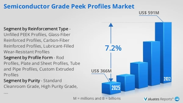
 Figure 26. Global Semiconductor Grade PEEK Profiles Production Value (US$ Million), 2021 vs 2025 vs 2032
 Figure 27. Global Semiconductor Grade PEEK Profiles Production Value (US$ Million), 2021–2032
 Figure 28. Global Semiconductor Grade PEEK Profiles Production Capacity (Tons), 2021–2032
 Figure 29. Global Semiconductor Grade PEEK Profiles Production (Tons), 2021–2032
 Figure 30. Global Semiconductor Grade PEEK Profiles Average Price (US$/kg), 2021–2032
 Figure 31. Semiconductor Grade PEEK Profiles Report Years Considered
 Figure 32. Semiconductor Grade PEEK Profiles Production Share by Manufacturers in 2025
 Figure 33. Global Semiconductor Grade PEEK Profiles Production Value Share by Manufacturers (2025)
 Figure 34. Semiconductor Grade PEEK Profiles Market Share by Company Type (Tier 1, Tier 2, and Tier 3): 2021 vs 2025
 Figure 35. Top 5 and Top 10 Global Players: Market Share by Semiconductor Grade PEEK Profiles Revenue in 2025
 Figure 36. Global Semiconductor Grade PEEK Profiles Production Value by Region: 2021 vs 2025 vs 2032 (US$ Million)
 Figure 37. Global Semiconductor Grade PEEK Profiles Production Value Market Share by Region: 2021 vs 2025 vs 2032
 Figure 38. Global Semiconductor Grade PEEK Profiles Production Comparison by Region: 2021 vs 2025 vs 2032 (Tons)
 Figure 39. Global Semiconductor Grade PEEK Profiles Production Market Share by Region: 2021 vs 2025 vs 2032
 Figure 40. North America Semiconductor Grade PEEK Profiles Production Value (US$ Million) Growth Rate (2021–2032)
 Figure 41. Europe Semiconductor Grade PEEK Profiles Production Value (US$ Million) Growth Rate (2021–2032)
 Figure 42. China Semiconductor Grade PEEK Profiles Production Value (US$ Million) Growth Rate (2021–2032)
 Figure 43. Japan Semiconductor Grade PEEK Profiles Production Value (US$ Million) Growth Rate (2021–2032)
 Figure 44. Global Semiconductor Grade PEEK Profiles Consumption by Region: 2021 vs 2025 vs 2032 (Tons)
 Figure 45. Global Semiconductor Grade PEEK Profiles Consumption Market Share by Region: 2021 vs 2025 vs 2032
 Figure 46. North America Semiconductor Grade PEEK Profiles Consumption and Growth Rate (Tons), 2021–2032
 Figure 47. North America Semiconductor Grade PEEK Profiles Consumption Market Share by Country (2021–2032)
 Figure 48. U.S. Semiconductor Grade PEEK Profiles Consumption and Growth Rate (Tons), 2021–2032
 Figure 49. Canada Semiconductor Grade PEEK Profiles Consumption and Growth Rate (Tons), 2021–2032
 Figure 50. Europe Semiconductor Grade PEEK Profiles Consumption and Growth Rate (Tons), 2021–2032
 Figure 51. Europe Semiconductor Grade PEEK Profiles Consumption Market Share by Country (2021–2032)
 Figure 52. Germany Semiconductor Grade PEEK Profiles Consumption and Growth Rate (Tons), 2021–2032
 Figure 53. France Semiconductor Grade PEEK Profiles Consumption and Growth Rate (Tons), 2021–2032
 Figure 54. U.K. Semiconductor Grade PEEK Profiles Consumption and Growth Rate (Tons), 2021–2032
 Figure 55. Italy Semiconductor Grade PEEK Profiles Consumption and Growth Rate (Tons), 2021–2032
 Figure 56. Russia Semiconductor Grade PEEK Profiles Consumption and Growth Rate (Tons), 2021–2032
 Figure 57. Asia Pacific Semiconductor Grade PEEK Profiles Consumption and Growth Rate (Tons), 2021–2032
 Figure 58. Asia Pacific Semiconductor Grade PEEK Profiles Consumption Market Share by Region (2021–2032)
 Figure 59. China Semiconductor Grade PEEK Profiles Consumption and Growth Rate (Tons), 2021–2032
 Figure 60. Japan Semiconductor Grade PEEK Profiles Consumption and Growth Rate (Tons), 2021–2032
 Figure 61. South Korea Semiconductor Grade PEEK Profiles Consumption and Growth Rate (Tons), 2021–2032
 Figure 62. China Taiwan Semiconductor Grade PEEK Profiles Consumption and Growth Rate (Tons), 2021–2032
 Figure 63. Southeast Asia Semiconductor Grade PEEK Profiles Consumption and Growth Rate (Tons), 2021–2032
 Figure 64. India Semiconductor Grade PEEK Profiles Consumption and Growth Rate (Tons), 2021–2032
 Figure 65. Latin America, Middle East & Africa Semiconductor Grade PEEK Profiles Consumption and Growth Rate (Tons), 2021–2032
 Figure 66. Latin America, Middle East & Africa Semiconductor Grade PEEK Profiles Consumption Market Share by Country (2021–2032)
 Figure 67. Mexico Semiconductor Grade PEEK Profiles Consumption and Growth Rate (Tons), 2021–2032
 Figure 68. Brazil Semiconductor Grade PEEK Profiles Consumption and Growth Rate (Tons), 2021–2032
 Figure 69. Turkey Semiconductor Grade PEEK Profiles Consumption and Growth Rate (Tons), 2021–2032
 Figure 70. GCC Countries Semiconductor Grade PEEK Profiles Consumption and Growth Rate (Tons), 2021–2032
 Figure 71. Global Production Market Share of Semiconductor Grade PEEK Profiles by Profile Form (2021–2032)
 Figure 72. Global Production Value Market Share of Semiconductor Grade PEEK Profiles by Profile Form (2021–2032)
 Figure 73. Global Semiconductor Grade PEEK Profiles Price (US$/kg) by Profile Form (2021–2032)
 Figure 74. Global Production Market Share of Semiconductor Grade PEEK Profiles by Application (2021–2032)
 Figure 75. Global Production Value Market Share of Semiconductor Grade PEEK Profiles by Application (2021–2032)
 Figure 76. Global Semiconductor Grade PEEK Profiles Price (US$/kg) by Application (2021–2032)
 Figure 77. Semiconductor Grade PEEK Profiles Value Chain
 Figure 78. Channels of Distribution (Direct Vs Distribution)
 Figure 79. Bottom-up and Top-down Approaches for This Report
 Figure 80. Data Triangulation
SELECT A FORMAT
Added to Cart
Electronic

$2900

Single User License
Electronic

$4350

Multi User License
Electronic

$5800

Enterprise License
Add to Cart
Buy Now (15% Discount)

OUR CUSTOMER

SecuX Technology Inc