FEATURED COMPANIES
Pure Wafer
RS Technologies
Sumco
GlobalWafers
Test Grade Wafers Market Size
The global Test Grade Wafers market was valued at US$ 1864 million in 2025 and is anticipated to reach US$ 2413 million by 2032, at a CAGR of 6.3% from 2026 to 2032.
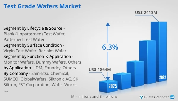
Test Grade Wafers Market
The 2025 U.S. tariff policies introduce profound uncertainty into the global economic landscape. This report critically examines the implications of recent tariff adjustments and international strategic countermeasures on Test Grade Wafers competitive dynamics, regional economic interdependencies, and supply chain reconfigurations.
In fab operations, a Test Wafer is a non-product wafer used to qualify tools and processes, tune recipes, explore process windows (DOE), replicate excursions, and support metrology/calibration—i.e., it does not ship as product but protects yield and accelerates ramp. IRDS/Factory Integration explicitly frames typical non-production wafers as test wafers, monitor wafers, and calibration wafers, and treats them as an operational lever because they consume production tool capacity and must be managed as part of factory performance. Practically, Test Wafers overlap with Monitor Wafers in that both can run representative steps and generate measurable outputs (film thickness, etch rate/depth, particles/contamination), but Test Wafers skew toward engineering qualification and recipe development, while Monitor Wafers skew toward SPC/ongoing process control. Common supply forms include test-grade virgin wafers, film-conditioned wafers (e.g., pre-oxide/nitride), patterned/calibration test wafers, and reclaimed wafers used repeatedly to reduce cost.
Test Wafers are predominantly single-crystal silicon, configured to emulate production responses with controlled specifications: CZ or FZ crystal routes, selected orientation/doping/resistivity windows, and surface/structure options such as polished/non-polished and epitaxial variants. A major wafer maker’s portfolio description highlights coverage from non-polished to epitaxial wafers up to 300 mm and explains that CZ and FZ ingots are used to obtain crystal properties tailored to customer applications—an approach directly aligned with test-wafer configurability. The differentiators are therefore mechanical/geometry stability and surface quality (TTV, bow/warp, edge/surface condition, baseline particle/metal contamination), because these drive measurement comparability and drift sensitivity. Reclaim is a core cost lever: reclaim removes unwanted films/material via dry/wet steps, then polishes and cleans to restore the silicon surface, while repeated cycles progressively thin the wafer and eventually force replacement. Leading reclaim suppliers emphasize advanced stripping, polishing/cleaning, and metal-impurity (e.g., copper) removal plus minimum-etch approaches to extend reclaim cycles and achieve cleanliness comparable to new wafers.
The ecosystem is typically three-tiered: (1) wafer manufacturers supplying test-grade virgin and certain customized specs; (2) reclaim and value-add providers supplying reclaimed test/monitor/dummy wafers and optional value-add films/finishing—SEMI’s member directory description for WRS Materials lists wafer reclaiming, thermal oxidation, sputtered/deposited films, grinding and polishing, plus Prime and Test grade offerings; and (3) patterned/calibration wafer providers delivering IP-neutral metrology/process artifacts (e.g., AMAG7 patterned calibration wafers). Over 2020–2025, test wafer demand is structurally supported by rising metrology intensity and tighter process windows in advanced manufacturing, while cost/sustainability pressures accelerate reclaim reuse—RS Technologies explicitly notes that fabs use monitor and dummy wafers for testing and trial processing and reuse them after precision reclaim; Nippon Chemi-Con similarly defines reclaimed wafers as dummy wafers used for testing/checking equipment and then re-polished for reuse. In parallel, the industry’s shift toward larger wafer diameters (and the phase-out of small-diameter capacity in some regions) reinforces a trend toward 200/300 mm test wafers with tighter geometry control; Reuters’ report on Siltronic’s plan to cease small-diameter wafer production by 2025 is consistent with this demand migration.
This report delivers a comprehensive overview of the global Test Grade Wafers market, with both quantitative and qualitative analyses, to help readers develop growth strategies, assess the competitive landscape, evaluate their position in the current market, and make informed business decisions regarding Test Grade Wafers. The Test Grade Wafers market size, estimates, and forecasts are provided in terms of output/shipments (K Pcs) and revenue (US$ millions), with 2025 as the base year and historical and forecast data for 2021–2032.
The report segments the global Test Grade Wafers market comprehensively. Regional market sizes by Function & Application, by Application, by Surface Condition, and by company are also provided. For deeper insight, the report profiles the competitive landscape, key competitors, and their respective market rankings, and discusses technological trends and new product developments.
This report will assist Test Grade Wafers manufacturers, new entrants, and companies across the industry value chain with information on revenues, production, and average prices for the overall market and its sub-segments, by company, by Function & Application, by Application, and by region.
Market Segmentation
Scope of Test Grade Wafers Market Report
| Report Metric |
Details |
| Report Name |
Test Grade Wafers Market |
| Accounted market size in 2025 |
US$ 1864 million |
| Forecasted market size in 2032 |
US$ 2413 million |
| CAGR |
6.3% |
| Base Year |
2025 |
| Forecasted years |
2026 - 2032 |
| Segment by Function & Application |
- Monitor Wafers
- Dummy Wafers
- Others
|
| Segment by Surface Condition |
- Virgin Test Wafer
- Reclaim Wafer
|
| Segment by Lifecycle & Source |
- Blank (Unpatterned) Test Wafer
- Patterned Test Wafer
|
| by Application |
|
| Production by Region |
- North America
- Europe
- China
- Japan
- South Korea
- China Taiwan
|
| Consumption by Region |
- North America (United States, Canada)
- Europe (Germany, France, UK, Italy, Russia)
- Asia-Pacific (China, Japan, South Korea, Taiwan)
- Southeast Asia (India)
- Latin America (Mexico, Brazil)
|
| By Company |
Shin-Etsu Chemical, SUMCO, GlobalWafers, Siltronic AG, SK Siltron, FST Corporation, Wafer Works Corporation, National Silicon Industry Group (NSIG), Zhonghuan Advanced Semiconductor Materials, Hangzhou Lion Microelectronics, Hangzhou Semiconductor Wafer, GRINM Semiconductor Materials, Shanghai Advanced Silicon Technology (AST), Xi'an ESWIN Material Technology, RS Technologies, Kinik, Phoenix Silicon International, Hamada Rectech, Mimasu Semiconductor Industry, GST, Scientech, Pure Wafer, TOPCO Scientific Co. LTD |
| Forecast units |
USD million in value |
| Report coverage |
Revenue and volume forecast, company share, competitive landscape, growth factors and trends |
Chapter Outline
- Chapter 1: Defines the scope of the report and presents an executive summary of market segments (by Function & Application, by Application, by Surface Condition, etc.), including the size of each segment and its future growth potential. It offers a high-level view of the current market and its likely evolution in the short, medium, and long term.
- Chapter 2: Provides a detailed analysis of the competitive landscape for Test Grade Wafers manufacturers, including prices, production, value-based market shares, latest development plans, and information on mergers and acquisitions.
- Chapter 3: Examines Test Grade Wafers production/output and value by region and country, providing a quantitative assessment of market size and growth potential for each region over the next six years.
- Chapter 4: Analyzes Test Grade Wafers consumption at the regional and country levels. It quantifies market size and growth potential for each region and its key countries, and outlines market development, outlook, addressable space, and national production.
- Chapter 5: Analyzes market segments by Function & Application, covering the size and growth potential of each segment to help readers identify “blue ocean” opportunities.
- Chapter 6: Analyzes market segments by Application, covering the size and growth potential of each segment to help readers identify “blue ocean” opportunities in downstream markets.
- Chapter 7: Profiles key players, detailing the fundamentals of major companies, including product production/output, value, price, gross margin, product portfolio/introductions, and recent developments.
- Chapter 8: Reviews the industry value chain, including upstream and downstream segments.
- Chapter 9: Discusses market dynamics and recent developments, including drivers, restraints, challenges and risks for manufacturers, U.S. Tariffs and relevant policy analysis.
- Chapter 10: Summarizes the key findings and conclusions of the report.
FAQ for this report
How fast is Test Grade Wafers Market growing?
Ans: The Test Grade Wafers Market witnessing a CAGR of 6.3% during the forecast period 2026-2032.
What is the Test Grade Wafers Market size in 2032?
Ans: The Test Grade Wafers Market size in 2032 will be US$ 2413 million.
Who are the main players in the Test Grade Wafers Market report?
Ans: The main players in the Test Grade Wafers Market are Shin-Etsu Chemical, SUMCO, GlobalWafers, Siltronic AG, SK Siltron, FST Corporation, Wafer Works Corporation, National Silicon Industry Group (NSIG), Zhonghuan Advanced Semiconductor Materials, Hangzhou Lion Microelectronics, Hangzhou Semiconductor Wafer, GRINM Semiconductor Materials, Shanghai Advanced Silicon Technology (AST), Xi'an ESWIN Material Technology, RS Technologies, Kinik, Phoenix Silicon International, Hamada Rectech, Mimasu Semiconductor Industry, GST, Scientech, Pure Wafer, TOPCO Scientific Co. LTD
What are the Application segmentation covered in the Test Grade Wafers Market report?
Ans: The Applications covered in the Test Grade Wafers Market report are IDM, Foundry, Others