0
U.S. (TOLL FREE)
+1 (315) 215-3225
Automative

0
U.S. (TOLL FREE)
+1 (315) 215-3225
Global Semiconductor Wafer Microscope Market Research Report 2025
Published Date: April 2025
|
Report Code: QYRE-Auto-20N11786
Home | Market Reports | Science
Global Semiconductor Wafer Microscope Market Research Report 2022
BUY CHAPTERS

Global Semiconductor Wafer Microscope Market Research Report 2025

Code: QYRE-Auto-20N11786
Report
April 2025
Pages:120
QYResearch
Buy Now with 15% Discount
DESCRIPTION
TABLE OF CONTENT
TABLES & FIGURES

Semiconductor Wafer Microscope Market Size

The global market for Semiconductor Wafer Microscope was valued at US$ 941 million in the year 2024 and is projected to reach a revised size of US$ 1606 million by 2031, growing at a CAGR of 7.6% during the forecast period.

Semiconductor Wafer Microscope Market

Semiconductor Wafer Microscope Market

Semiconductor inspection runs through the entire semiconductor process, that is, the front-end and back-end. Semiconductor inspection includes optical inspection, electron beam inspection and X-ray measurement. It mainly detects whether there are abnormal quality conditions on the surface of the wafer or in the circuit structure, such as scratches, particle contamination, graphic errors and other defects. Different inspection technologies have obvious differences, mainly reflected in accuracy, speed and inspection purposes.
Semiconductor inspection types include patterned, non-patterned and mask inspection. Among them, patterned defect inspection is divided into bright field and dark field inspection. Both are analyzed through optical signals. The difference is that the bright field is a vertically reflected light signal, while the dark field is a scattered light signal.
Microscopes used in semiconductor manufacturing processes can be divided into inspection microscopes and metrology microscopes according to their uses.
Among them, inspection microscopes mainly include optical microscopes and electron beam scanning microscopes (SEM). The main function is to inspection the graphics and defects on the surface of the wafer.
Metrology microscopes include CD-SEM, atomic force microscope (AFM), etc. Among them, CD-SEM is used to measure the key dimensions of semiconductor devices (such as line width, spacing, etc.); AFM provides nanometer-level precision dimensional measurement by measuring surface morphology and height.
The global wafer inspection microscope manufacturers mainly include Leica, Motic, Evident Scientific, Hitachi High-Tech, Applied Materials, ZEISS, Jeol Ltd, Nikon, Advantest, Park Systems, etc. In 2023, the market share of the top ten manufacturers in the world exceeded 70%. Among them, CD-SEM is dominated by Hitachi and Applied Materials; AFM is dominated by Park Systems and Bruker; optical microscopes are dominated by Leica, Nikon and Evident Scientific.
The demand for wafer inspection microscopes is closely related to the overall development of semiconductors. The global semiconductor industry is huge. According to the data of the World Semiconductor Trade Statistics Organization (WSTS), the overall scale of the global semiconductor industry in 2023 is US$526.8 billion, a year-on-year decrease of 8.2% compared with 2022. Among them, in the manufacturing link, according to the calculation of our company's research team, the global market size of semiconductor chip manufacturing in 2023 will be US$250 billion, of which pure foundry revenue accounts for about 45% and IDM accounts for 55%. In the next few years, it is expected that the share of foundry companies will further increase. In the coming years, as the semiconductor industry continues to grow, the demand for wafer inspection microscopes will be further increased.

Report Scope

This report aims to provide a comprehensive presentation of the global market for Semiconductor Wafer Microscope, with both quantitative and qualitative analysis, to help readers develop business/growth strategies, assess the market competitive situation, analyze their position in the current marketplace, and make informed business decisions regarding Semiconductor Wafer Microscope.
The 2025 U.S. tariff policies introduce profound uncertainty into the global economic landscape. This report critically examines the implications of recent tariff adjustments and international strategic countermeasures on Semiconductor Wafer Microscope competitive dynamics, regional economic interdependencies, and supply chain reconfigurations.
The Semiconductor Wafer Microscope market size, estimations, and forecasts are provided in terms of output/shipments (Units) and revenue ($ millions), considering 2024 as the base year, with history and forecast data for the period from 2020 to 2031. This report segments the global Semiconductor Wafer Microscope market comprehensively. Regional market sizes, concerning products by Type, by Application, and by players, are also provided.
For a more in-depth understanding of the market, the report provides profiles of the competitive landscape, key competitors, and their respective market ranks. The report also discusses technological trends and new product developments.
The report will help the Semiconductor Wafer Microscope manufacturers, new entrants, and industry chain related companies in this market with information on the revenues, production, and average price for the overall market and the sub-segments across the different segments, by company, by Type, by Application, and by regions.

Scope of Semiconductor Wafer Microscope Market Report

Report Metric Details
Report Name Semiconductor Wafer Microscope Market
Accounted market size in year US$ 941 million
Forecasted market size in 2031 US$ 1606 million
CAGR 7.6%
Base Year year
Forecasted years 2025 - 2031
Segment by Type
  • Optical Microscope
  • FIB-SEM & TEM
  • AFM
  • CD-SEM
Segment by Application
  • 300mm Wafer
  • 200mm Wafer
  • Others
Production by Region
  • North America
  • Europe
  • China
  • Japan
Consumption by Region
  • North America (United States, Canada)
  • Europe (Germany, France, UK, Italy, Russia)
  • Asia-Pacific (China, Japan, South Korea, Taiwan)
  • Southeast Asia (India)
  • Latin America (Mexico, Brazil)
By Company Leica Microsystems, Motic, Evident Scientific, Nikon, Thermo Fisher Scientific, Hitachi High-Technologies Corporation, Jeol Ltd, Tescan Group, Hirox, ZEISS, Applied Materials, Advantest, Holon, TCK, Dongfang Jingyuan Electron, Park Systems, Bruker, Oxford Instruments, NT-MDT, Horiba, Nanosurf, Nanonics Imaging, Attocube Systems AG, Concept Scientific Instruments, NanoMagnetics Instruments
Forecast units USD million in value
Report coverage Revenue and volume forecast, company share, competitive landscape, growth factors and trends

Chapter Outline

  • Chapter 1: Introduces the report scope of the report, executive summary of different market segments (by region, by Type, by Application, etc), including the market size of each market segment, future development potential, and so on. It offers a high-level view of the current state of the market and its likely evolution in the short to mid-term, and long term.
  • Chapter 2: Detailed analysis of Semiconductor Wafer Microscope manufacturers competitive landscape, price, production and value market share, latest development plan, merger, and acquisition information, etc.
  • Chapter 3: Production/output, value of Semiconductor Wafer Microscope by region/country. It provides a quantitative analysis of the market size and development potential of each region in the next six years.
  • Chapter 4: Consumption of Semiconductor Wafer Microscope in regional level and country level. It provides a quantitative analysis of the market size and development potential of each region and its main countries and introduces the market development, future development prospects, market space, and production of each country in the world.
  • Chapter 5: Provides the analysis of various market segments by Type, covering the market size and development potential of each market segment, to help readers find the blue ocean market in different market segments.
  • Chapter 6: Provides the analysis of various market segments by Application, covering the market size and development potential of each market segment, to help readers find the blue ocean market in different downstream markets.
  • Chapter 7: Provides profiles of key players, introducing the basic situation of the main companies in the market in detail, including product production/output, value, price, gross margin, product introduction, recent development, etc.
  • Chapter 8: Analysis of industrial chain, including the upstream and downstream of the industry.
  • Chapter 9: Introduces the market dynamics, latest developments of the market, the driving factors and restrictive factors of the market, the challenges and risks faced by manufacturers in the industry, and the analysis of relevant policies in the industry.
  • Chapter 10: The main points and conclusions of the report.

FAQ for this report

How fast is Semiconductor Wafer Microscope Market growing?

Ans: The Semiconductor Wafer Microscope Market witnessing a CAGR of 7.6% during the forecast period 2025-2031.

What is the Semiconductor Wafer Microscope Market size in 2031?

Ans: The Semiconductor Wafer Microscope Market size in 2031 will be US$ 1606 million.

What is the market share of major companies in Semiconductor Wafer Microscope Market?

Ans: In 2023, the market share of the top ten manufacturers in the world exceeded 70%.

Who are the main players in the Semiconductor Wafer Microscope Market report?

Ans: The main players in the Semiconductor Wafer Microscope Market are Leica Microsystems, Motic, Evident Scientific, Nikon, Thermo Fisher Scientific, Hitachi High-Technologies Corporation, Jeol Ltd, Tescan Group, Hirox, ZEISS, Applied Materials, Advantest, Holon, TCK, Dongfang Jingyuan Electron, Park Systems, Bruker, Oxford Instruments, NT-MDT, Horiba, Nanosurf, Nanonics Imaging, Attocube Systems AG, Concept Scientific Instruments, NanoMagnetics Instruments

What are the Application segmentation covered in the Semiconductor Wafer Microscope Market report?

Ans: The Applications covered in the Semiconductor Wafer Microscope Market report are 300mm Wafer, 200mm Wafer, Others

What are the Type segmentation covered in the Semiconductor Wafer Microscope Market report?

Ans: The Types covered in the Semiconductor Wafer Microscope Market report are Optical Microscope, FIB-SEM & TEM, AFM, CD-SEM

1 Semiconductor Wafer Microscope Market Overview
1.1 Product Definition
1.2 Semiconductor Wafer Microscope by Type
1.2.1 Global Semiconductor Wafer Microscope Market Value Growth Rate Analysis by Type: 2024 VS 2031
1.2.2 Optical Microscope
1.2.3 FIB-SEM & TEM
1.2.4 AFM
1.2.5 CD-SEM
1.3 Semiconductor Wafer Microscope by Application
1.3.1 Global Semiconductor Wafer Microscope Market Value Growth Rate Analysis by Application: 2024 VS 2031
1.3.2 300mm Wafer
1.3.3 200mm Wafer
1.3.4 Others
1.4 Global Market Growth Prospects
1.4.1 Global Semiconductor Wafer Microscope Production Value Estimates and Forecasts (2020-2031)
1.4.2 Global Semiconductor Wafer Microscope Production Capacity Estimates and Forecasts (2020-2031)
1.4.3 Global Semiconductor Wafer Microscope Production Estimates and Forecasts (2020-2031)
1.4.4 Global Semiconductor Wafer Microscope Market Average Price Estimates and Forecasts (2020-2031)
1.5 Assumptions and Limitations
2 Market Competition by Manufacturers
2.1 Global Semiconductor Wafer Microscope Production Market Share by Manufacturers (2020-2025)
2.2 Global Semiconductor Wafer Microscope Production Value Market Share by Manufacturers (2020-2025)
2.3 Global Key Players of Semiconductor Wafer Microscope, Industry Ranking, 2023 VS 2024
2.4 Global Semiconductor Wafer Microscope Company Type and Market Share by Company Type (Tier 1, Tier 2, and Tier 3)
2.5 Global Semiconductor Wafer Microscope Average Price by Manufacturers (2020-2025)
2.6 Global Key Manufacturers of Semiconductor Wafer Microscope, Manufacturing Base Distribution and Headquarters
2.7 Global Key Manufacturers of Semiconductor Wafer Microscope, Product Offered and Application
2.8 Global Key Manufacturers of Semiconductor Wafer Microscope, Date of Enter into This Industry
2.9 Semiconductor Wafer Microscope Market Competitive Situation and Trends
2.9.1 Semiconductor Wafer Microscope Market Concentration Rate
2.9.2 Global 5 and 10 Largest Semiconductor Wafer Microscope Players Market Share by Revenue
2.10 Mergers & Acquisitions, Expansion
3 Semiconductor Wafer Microscope Production by Region
3.1 Global Semiconductor Wafer Microscope Production Value Estimates and Forecasts by Region: 2020 VS 2024 VS 2031
3.2 Global Semiconductor Wafer Microscope Production Value by Region (2020-2031)
3.2.1 Global Semiconductor Wafer Microscope Production Value by Region (2020-2025)
3.2.2 Global Forecasted Production Value of Semiconductor Wafer Microscope by Region (2026-2031)
3.3 Global Semiconductor Wafer Microscope Production Estimates and Forecasts by Region: 2020 VS 2024 VS 2031
3.4 Global Semiconductor Wafer Microscope Production Volume by Region (2020-2031)
3.4.1 Global Semiconductor Wafer Microscope Production by Region (2020-2025)
3.4.2 Global Forecasted Production of Semiconductor Wafer Microscope by Region (2026-2031)
3.5 Global Semiconductor Wafer Microscope Market Price Analysis by Region (2020-2025)
3.6 Global Semiconductor Wafer Microscope Production and Value, Year-over-Year Growth
3.6.1 North America Semiconductor Wafer Microscope Production Value Estimates and Forecasts (2020-2031)
3.6.2 Europe Semiconductor Wafer Microscope Production Value Estimates and Forecasts (2020-2031)
3.6.3 China Semiconductor Wafer Microscope Production Value Estimates and Forecasts (2020-2031)
3.6.4 Japan Semiconductor Wafer Microscope Production Value Estimates and Forecasts (2020-2031)
4 Semiconductor Wafer Microscope Consumption by Region
4.1 Global Semiconductor Wafer Microscope Consumption Estimates and Forecasts by Region: 2020 VS 2024 VS 2031
4.2 Global Semiconductor Wafer Microscope Consumption by Region (2020-2031)
4.2.1 Global Semiconductor Wafer Microscope Consumption by Region (2020-2025)
4.2.2 Global Semiconductor Wafer Microscope Forecasted Consumption by Region (2026-2031)
4.3 North America
4.3.1 North America Semiconductor Wafer Microscope Consumption Growth Rate by Country: 2020 VS 2024 VS 2031
4.3.2 North America Semiconductor Wafer Microscope Consumption by Country (2020-2031)
4.3.3 U.S.
4.3.4 Canada
4.4 Europe
4.4.1 Europe Semiconductor Wafer Microscope Consumption Growth Rate by Country: 2020 VS 2024 VS 2031
4.4.2 Europe Semiconductor Wafer Microscope Consumption by Country (2020-2031)
4.4.3 Germany
4.4.4 France
4.4.5 U.K.
4.4.6 Italy
4.4.7 Netherlands
4.5 Asia Pacific
4.5.1 Asia Pacific Semiconductor Wafer Microscope Consumption Growth Rate by Region: 2020 VS 2024 VS 2031
4.5.2 Asia Pacific Semiconductor Wafer Microscope Consumption by Region (2020-2031)
4.5.3 China
4.5.4 Japan
4.5.5 South Korea
4.5.6 China Taiwan
4.5.7 Southeast Asia
4.5.8 India
4.6 Latin America, Middle East & Africa
4.6.1 Latin America, Middle East & Africa Semiconductor Wafer Microscope Consumption Growth Rate by Country: 2020 VS 2024 VS 2031
4.6.2 Latin America, Middle East & Africa Semiconductor Wafer Microscope Consumption by Country (2020-2031)
4.6.3 Mexico
4.6.4 Brazil
4.6.5 Turkey
4.6.6 GCC Countries
5 Segment by Type
5.1 Global Semiconductor Wafer Microscope Production by Type (2020-2031)
5.1.1 Global Semiconductor Wafer Microscope Production by Type (2020-2025)
5.1.2 Global Semiconductor Wafer Microscope Production by Type (2026-2031)
5.1.3 Global Semiconductor Wafer Microscope Production Market Share by Type (2020-2031)
5.2 Global Semiconductor Wafer Microscope Production Value by Type (2020-2031)
5.2.1 Global Semiconductor Wafer Microscope Production Value by Type (2020-2025)
5.2.2 Global Semiconductor Wafer Microscope Production Value by Type (2026-2031)
5.2.3 Global Semiconductor Wafer Microscope Production Value Market Share by Type (2020-2031)
5.3 Global Semiconductor Wafer Microscope Price by Type (2020-2031)
6 Segment by Application
6.1 Global Semiconductor Wafer Microscope Production by Application (2020-2031)
6.1.1 Global Semiconductor Wafer Microscope Production by Application (2020-2025)
6.1.2 Global Semiconductor Wafer Microscope Production by Application (2026-2031)
6.1.3 Global Semiconductor Wafer Microscope Production Market Share by Application (2020-2031)
6.2 Global Semiconductor Wafer Microscope Production Value by Application (2020-2031)
6.2.1 Global Semiconductor Wafer Microscope Production Value by Application (2020-2025)
6.2.2 Global Semiconductor Wafer Microscope Production Value by Application (2026-2031)
6.2.3 Global Semiconductor Wafer Microscope Production Value Market Share by Application (2020-2031)
6.3 Global Semiconductor Wafer Microscope Price by Application (2020-2031)
7 Key Companies Profiled
7.1 Leica Microsystems
7.1.1 Leica Microsystems Semiconductor Wafer Microscope Company Information
7.1.2 Leica Microsystems Semiconductor Wafer Microscope Product Portfolio
7.1.3 Leica Microsystems Semiconductor Wafer Microscope Production, Value, Price and Gross Margin (2020-2025)
7.1.4 Leica Microsystems Main Business and Markets Served
7.1.5 Leica Microsystems Recent Developments/Updates
7.2 Motic
7.2.1 Motic Semiconductor Wafer Microscope Company Information
7.2.2 Motic Semiconductor Wafer Microscope Product Portfolio
7.2.3 Motic Semiconductor Wafer Microscope Production, Value, Price and Gross Margin (2020-2025)
7.2.4 Motic Main Business and Markets Served
7.2.5 Motic Recent Developments/Updates
7.3 Evident Scientific
7.3.1 Evident Scientific Semiconductor Wafer Microscope Company Information
7.3.2 Evident Scientific Semiconductor Wafer Microscope Product Portfolio
7.3.3 Evident Scientific Semiconductor Wafer Microscope Production, Value, Price and Gross Margin (2020-2025)
7.3.4 Evident Scientific Main Business and Markets Served
7.3.5 Evident Scientific Recent Developments/Updates
7.4 Nikon
7.4.1 Nikon Semiconductor Wafer Microscope Company Information
7.4.2 Nikon Semiconductor Wafer Microscope Product Portfolio
7.4.3 Nikon Semiconductor Wafer Microscope Production, Value, Price and Gross Margin (2020-2025)
7.4.4 Nikon Main Business and Markets Served
7.4.5 Nikon Recent Developments/Updates
7.5 Thermo Fisher Scientific
7.5.1 Thermo Fisher Scientific Semiconductor Wafer Microscope Company Information
7.5.2 Thermo Fisher Scientific Semiconductor Wafer Microscope Product Portfolio
7.5.3 Thermo Fisher Scientific Semiconductor Wafer Microscope Production, Value, Price and Gross Margin (2020-2025)
7.5.4 Thermo Fisher Scientific Main Business and Markets Served
7.5.5 Thermo Fisher Scientific Recent Developments/Updates
7.6 Hitachi High-Technologies Corporation
7.6.1 Hitachi High-Technologies Corporation Semiconductor Wafer Microscope Company Information
7.6.2 Hitachi High-Technologies Corporation Semiconductor Wafer Microscope Product Portfolio
7.6.3 Hitachi High-Technologies Corporation Semiconductor Wafer Microscope Production, Value, Price and Gross Margin (2020-2025)
7.6.4 Hitachi High-Technologies Corporation Main Business and Markets Served
7.6.5 Hitachi High-Technologies Corporation Recent Developments/Updates
7.7 Jeol Ltd
7.7.1 Jeol Ltd Semiconductor Wafer Microscope Company Information
7.7.2 Jeol Ltd Semiconductor Wafer Microscope Product Portfolio
7.7.3 Jeol Ltd Semiconductor Wafer Microscope Production, Value, Price and Gross Margin (2020-2025)
7.7.4 Jeol Ltd Main Business and Markets Served
7.7.5 Jeol Ltd Recent Developments/Updates
7.8 Tescan Group
7.8.1 Tescan Group Semiconductor Wafer Microscope Company Information
7.8.2 Tescan Group Semiconductor Wafer Microscope Product Portfolio
7.8.3 Tescan Group Semiconductor Wafer Microscope Production, Value, Price and Gross Margin (2020-2025)
7.8.4 Tescan Group Main Business and Markets Served
7.8.5 Tescan Group Recent Developments/Updates
7.9 Hirox
7.9.1 Hirox Semiconductor Wafer Microscope Company Information
7.9.2 Hirox Semiconductor Wafer Microscope Product Portfolio
7.9.3 Hirox Semiconductor Wafer Microscope Production, Value, Price and Gross Margin (2020-2025)
7.9.4 Hirox Main Business and Markets Served
7.9.5 Hirox Recent Developments/Updates
7.10 ZEISS
7.10.1 ZEISS Semiconductor Wafer Microscope Company Information
7.10.2 ZEISS Semiconductor Wafer Microscope Product Portfolio
7.10.3 ZEISS Semiconductor Wafer Microscope Production, Value, Price and Gross Margin (2020-2025)
7.10.4 ZEISS Main Business and Markets Served
7.10.5 ZEISS Recent Developments/Updates
7.11 Applied Materials
7.11.1 Applied Materials Semiconductor Wafer Microscope Company Information
7.11.2 Applied Materials Semiconductor Wafer Microscope Product Portfolio
7.11.3 Applied Materials Semiconductor Wafer Microscope Production, Value, Price and Gross Margin (2020-2025)
7.11.4 Applied Materials Main Business and Markets Served
7.11.5 Applied Materials Recent Developments/Updates
7.12 Advantest
7.12.1 Advantest Semiconductor Wafer Microscope Company Information
7.12.2 Advantest Semiconductor Wafer Microscope Product Portfolio
7.12.3 Advantest Semiconductor Wafer Microscope Production, Value, Price and Gross Margin (2020-2025)
7.12.4 Advantest Main Business and Markets Served
7.12.5 Advantest Recent Developments/Updates
7.13 Holon
7.13.1 Holon Semiconductor Wafer Microscope Company Information
7.13.2 Holon Semiconductor Wafer Microscope Product Portfolio
7.13.3 Holon Semiconductor Wafer Microscope Production, Value, Price and Gross Margin (2020-2025)
7.13.4 Holon Main Business and Markets Served
7.13.5 Holon Recent Developments/Updates
7.14 TCK
7.14.1 TCK Semiconductor Wafer Microscope Company Information
7.14.2 TCK Semiconductor Wafer Microscope Product Portfolio
7.14.3 TCK Semiconductor Wafer Microscope Production, Value, Price and Gross Margin (2020-2025)
7.14.4 TCK Main Business and Markets Served
7.14.5 TCK Recent Developments/Updates
7.15 Dongfang Jingyuan Electron
7.15.1 Dongfang Jingyuan Electron Semiconductor Wafer Microscope Company Information
7.15.2 Dongfang Jingyuan Electron Semiconductor Wafer Microscope Product Portfolio
7.15.3 Dongfang Jingyuan Electron Semiconductor Wafer Microscope Production, Value, Price and Gross Margin (2020-2025)
7.15.4 Dongfang Jingyuan Electron Main Business and Markets Served
7.15.5 Dongfang Jingyuan Electron Recent Developments/Updates
7.16 Park Systems
7.16.1 Park Systems Semiconductor Wafer Microscope Company Information
7.16.2 Park Systems Semiconductor Wafer Microscope Product Portfolio
7.16.3 Park Systems Semiconductor Wafer Microscope Production, Value, Price and Gross Margin (2020-2025)
7.16.4 Park Systems Main Business and Markets Served
7.16.5 Park Systems Recent Developments/Updates
7.17 Bruker
7.17.1 Bruker Semiconductor Wafer Microscope Company Information
7.17.2 Bruker Semiconductor Wafer Microscope Product Portfolio
7.17.3 Bruker Semiconductor Wafer Microscope Production, Value, Price and Gross Margin (2020-2025)
7.17.4 Bruker Main Business and Markets Served
7.17.5 Bruker Recent Developments/Updates
7.18 Oxford Instruments
7.18.1 Oxford Instruments Semiconductor Wafer Microscope Company Information
7.18.2 Oxford Instruments Semiconductor Wafer Microscope Product Portfolio
7.18.3 Oxford Instruments Semiconductor Wafer Microscope Production, Value, Price and Gross Margin (2020-2025)
7.18.4 Oxford Instruments Main Business and Markets Served
7.18.5 Oxford Instruments Recent Developments/Updates
7.19 NT-MDT
7.19.1 NT-MDT Semiconductor Wafer Microscope Company Information
7.19.2 NT-MDT Semiconductor Wafer Microscope Product Portfolio
7.19.3 NT-MDT Semiconductor Wafer Microscope Production, Value, Price and Gross Margin (2020-2025)
7.19.4 NT-MDT Main Business and Markets Served
7.19.5 NT-MDT Recent Developments/Updates
7.20 Horiba
7.20.1 Horiba Semiconductor Wafer Microscope Company Information
7.20.2 Horiba Semiconductor Wafer Microscope Product Portfolio
7.20.3 Horiba Semiconductor Wafer Microscope Production, Value, Price and Gross Margin (2020-2025)
7.20.4 Horiba Main Business and Markets Served
7.20.5 Horiba Recent Developments/Updates
7.21 Nanosurf
7.21.1 Nanosurf Semiconductor Wafer Microscope Company Information
7.21.2 Nanosurf Semiconductor Wafer Microscope Product Portfolio
7.21.3 Nanosurf Semiconductor Wafer Microscope Production, Value, Price and Gross Margin (2020-2025)
7.21.4 Nanosurf Main Business and Markets Served
7.21.5 Nanosurf Recent Developments/Updates
7.22 Nanonics Imaging
7.22.1 Nanonics Imaging Semiconductor Wafer Microscope Company Information
7.22.2 Nanonics Imaging Semiconductor Wafer Microscope Product Portfolio
7.22.3 Nanonics Imaging Semiconductor Wafer Microscope Production, Value, Price and Gross Margin (2020-2025)
7.22.4 Nanonics Imaging Main Business and Markets Served
7.22.5 Nanonics Imaging Recent Developments/Updates
7.23 Attocube Systems AG
7.23.1 Attocube Systems AG Semiconductor Wafer Microscope Company Information
7.23.2 Attocube Systems AG Semiconductor Wafer Microscope Product Portfolio
7.23.3 Attocube Systems AG Semiconductor Wafer Microscope Production, Value, Price and Gross Margin (2020-2025)
7.23.4 Attocube Systems AG Main Business and Markets Served
7.23.5 Attocube Systems AG Recent Developments/Updates
7.24 Concept Scientific Instruments
7.24.1 Concept Scientific Instruments Semiconductor Wafer Microscope Company Information
7.24.2 Concept Scientific Instruments Semiconductor Wafer Microscope Product Portfolio
7.24.3 Concept Scientific Instruments Semiconductor Wafer Microscope Production, Value, Price and Gross Margin (2020-2025)
7.24.4 Concept Scientific Instruments Main Business and Markets Served
7.24.5 Concept Scientific Instruments Recent Developments/Updates
7.25 NanoMagnetics Instruments
7.25.1 NanoMagnetics Instruments Semiconductor Wafer Microscope Company Information
7.25.2 NanoMagnetics Instruments Semiconductor Wafer Microscope Product Portfolio
7.25.3 NanoMagnetics Instruments Semiconductor Wafer Microscope Production, Value, Price and Gross Margin (2020-2025)
7.25.4 NanoMagnetics Instruments Main Business and Markets Served
7.25.5 NanoMagnetics Instruments Recent Developments/Updates
8 Industry Chain and Sales Channels Analysis
8.1 Semiconductor Wafer Microscope Industry Chain Analysis
8.2 Semiconductor Wafer Microscope Raw Material Supply Analysis
8.2.1 Key Raw Materials
8.2.2 Raw Materials Key Suppliers
8.3 Semiconductor Wafer Microscope Production Mode & Process Analysis
8.4 Semiconductor Wafer Microscope Sales and Marketing
8.4.1 Semiconductor Wafer Microscope Sales Channels
8.4.2 Semiconductor Wafer Microscope Distributors
8.5 Semiconductor Wafer Microscope Customer Analysis
9 Semiconductor Wafer Microscope Market Dynamics
9.1 Semiconductor Wafer Microscope Industry Trends
9.2 Semiconductor Wafer Microscope Market Drivers
9.3 Semiconductor Wafer Microscope Market Challenges
9.4 Semiconductor Wafer Microscope Market Restraints
10 Research Findings and Conclusion
11 Methodology and Data Source
11.1 Methodology/Research Approach
11.1.1 Research Programs/Design
11.1.2 Market Size Estimation
11.1.3 Market Breakdown and Data Triangulation
11.2 Data Source
11.2.1 Secondary Sources
11.2.2 Primary Sources
11.3 Author List
11.4 Disclaimer
List of Tables
 Table 1. Global Semiconductor Wafer Microscope Market Value by Type, (US$ Million) & (2024 VS 2031)
 Table 2. Global Semiconductor Wafer Microscope Market Value by Application, (US$ Million) & (2024 VS 2031)
 Table 3. Global Semiconductor Wafer Microscope Production Capacity (Units) by Manufacturers in 2024
 Table 4. Global Semiconductor Wafer Microscope Production by Manufacturers (2020-2025) & (Units)
 Table 5. Global Semiconductor Wafer Microscope Production Market Share by Manufacturers (2020-2025)
 Table 6. Global Semiconductor Wafer Microscope Production Value by Manufacturers (2020-2025) & (US$ Million)
 Table 7. Global Semiconductor Wafer Microscope Production Value Share by Manufacturers (2020-2025)
 Table 8. Global Key Players of Semiconductor Wafer Microscope, Industry Ranking, 2023 VS 2024
 Table 9. Company Type (Tier 1, Tier 2, and Tier 3) & (based on the Production Value in Semiconductor Wafer Microscope as of 2024)
 Table 10. Global Market Semiconductor Wafer Microscope Average Price by Manufacturers (K US$/Unit) & (2020-2025)
 Table 11. Global Key Manufacturers of Semiconductor Wafer Microscope, Manufacturing Base Distribution and Headquarters
 Table 12. Global Key Manufacturers of Semiconductor Wafer Microscope, Product Offered and Application
 Table 13. Global Key Manufacturers of Semiconductor Wafer Microscope, Date of Enter into This Industry
 Table 14. Global Semiconductor Wafer Microscope Manufacturers Market Concentration Ratio (CR5 and HHI)
 Table 15. Mergers & Acquisitions, Expansion Plans
 Table 16. Global Semiconductor Wafer Microscope Production Value by Region: 2020 VS 2024 VS 2031 (US$ Million)
 Table 17. Global Semiconductor Wafer Microscope Production Value (US$ Million) by Region (2020-2025)
 Table 18. Global Semiconductor Wafer Microscope Production Value Market Share by Region (2020-2025)
 Table 19. Global Semiconductor Wafer Microscope Production Value (US$ Million) Forecast by Region (2026-2031)
 Table 20. Global Semiconductor Wafer Microscope Production Value Market Share Forecast by Region (2026-2031)
 Table 21. Global Semiconductor Wafer Microscope Production Comparison by Region: 2020 VS 2024 VS 2031 (Units)
 Table 22. Global Semiconductor Wafer Microscope Production (Units) by Region (2020-2025)
 Table 23. Global Semiconductor Wafer Microscope Production Market Share by Region (2020-2025)
 Table 24. Global Semiconductor Wafer Microscope Production (Units) Forecast by Region (2026-2031)
 Table 25. Global Semiconductor Wafer Microscope Production Market Share Forecast by Region (2026-2031)
 Table 26. Global Semiconductor Wafer Microscope Market Average Price (K US$/Unit) by Region (2020-2025)
 Table 27. Global Semiconductor Wafer Microscope Market Average Price (K US$/Unit) by Region (2026-2031)
 Table 28. Global Semiconductor Wafer Microscope Consumption Growth Rate by Region: 2020 VS 2024 VS 2031 (Units)
 Table 29. Global Semiconductor Wafer Microscope Consumption by Region (2020-2025) & (Units)
 Table 30. Global Semiconductor Wafer Microscope Consumption Market Share by Region (2020-2025)
 Table 31. Global Semiconductor Wafer Microscope Forecasted Consumption by Region (2026-2031) & (Units)
 Table 32. Global Semiconductor Wafer Microscope Forecasted Consumption Market Share by Region (2026-2031)
 Table 33. North America Semiconductor Wafer Microscope Consumption Growth Rate by Country: 2020 VS 2024 VS 2031 (Units)
 Table 34. North America Semiconductor Wafer Microscope Consumption by Country (2020-2025) & (Units)
 Table 35. North America Semiconductor Wafer Microscope Consumption by Country (2026-2031) & (Units)
 Table 36. Europe Semiconductor Wafer Microscope Consumption Growth Rate by Country: 2020 VS 2024 VS 2031 (Units)
 Table 37. Europe Semiconductor Wafer Microscope Consumption by Country (2020-2025) & (Units)
 Table 38. Europe Semiconductor Wafer Microscope Consumption by Country (2026-2031) & (Units)
 Table 39. Asia Pacific Semiconductor Wafer Microscope Consumption Growth Rate by Region: 2020 VS 2024 VS 2031 (Units)
 Table 40. Asia Pacific Semiconductor Wafer Microscope Consumption by Region (2020-2025) & (Units)
 Table 41. Asia Pacific Semiconductor Wafer Microscope Consumption by Region (2026-2031) & (Units)
 Table 42. Latin America, Middle East & Africa Semiconductor Wafer Microscope Consumption Growth Rate by Country: 2020 VS 2024 VS 2031 (Units)
 Table 43. Latin America, Middle East & Africa Semiconductor Wafer Microscope Consumption by Country (2020-2025) & (Units)
 Table 44. Latin America, Middle East & Africa Semiconductor Wafer Microscope Consumption by Country (2026-2031) & (Units)
 Table 45. Global Semiconductor Wafer Microscope Production (Units) by Type (2020-2025)
 Table 46. Global Semiconductor Wafer Microscope Production (Units) by Type (2026-2031)
 Table 47. Global Semiconductor Wafer Microscope Production Market Share by Type (2020-2025)
 Table 48. Global Semiconductor Wafer Microscope Production Market Share by Type (2026-2031)
 Table 49. Global Semiconductor Wafer Microscope Production Value (US$ Million) by Type (2020-2025)
 Table 50. Global Semiconductor Wafer Microscope Production Value (US$ Million) by Type (2026-2031)
 Table 51. Global Semiconductor Wafer Microscope Production Value Market Share by Type (2020-2025)
 Table 52. Global Semiconductor Wafer Microscope Production Value Market Share by Type (2026-2031)
 Table 53. Global Semiconductor Wafer Microscope Price (K US$/Unit) by Type (2020-2025)
 Table 54. Global Semiconductor Wafer Microscope Price (K US$/Unit) by Type (2026-2031)
 Table 55. Global Semiconductor Wafer Microscope Production (Units) by Application (2020-2025)
 Table 56. Global Semiconductor Wafer Microscope Production (Units) by Application (2026-2031)
 Table 57. Global Semiconductor Wafer Microscope Production Market Share by Application (2020-2025)
 Table 58. Global Semiconductor Wafer Microscope Production Market Share by Application (2026-2031)
 Table 59. Global Semiconductor Wafer Microscope Production Value (US$ Million) by Application (2020-2025)
 Table 60. Global Semiconductor Wafer Microscope Production Value (US$ Million) by Application (2026-2031)
 Table 61. Global Semiconductor Wafer Microscope Production Value Market Share by Application (2020-2025)
 Table 62. Global Semiconductor Wafer Microscope Production Value Market Share by Application (2026-2031)
 Table 63. Global Semiconductor Wafer Microscope Price (K US$/Unit) by Application (2020-2025)
 Table 64. Global Semiconductor Wafer Microscope Price (K US$/Unit) by Application (2026-2031)
 Table 65. Leica Microsystems Semiconductor Wafer Microscope Company Information
 Table 66. Leica Microsystems Semiconductor Wafer Microscope Specification and Application
 Table 67. Leica Microsystems Semiconductor Wafer Microscope Production (Units), Value (US$ Million), Price (K US$/Unit) and Gross Margin (2020-2025)
 Table 68. Leica Microsystems Main Business and Markets Served
 Table 69. Leica Microsystems Recent Developments/Updates
 Table 70. Motic Semiconductor Wafer Microscope Company Information
 Table 71. Motic Semiconductor Wafer Microscope Specification and Application
 Table 72. Motic Semiconductor Wafer Microscope Production (Units), Value (US$ Million), Price (K US$/Unit) and Gross Margin (2020-2025)
 Table 73. Motic Main Business and Markets Served
 Table 74. Motic Recent Developments/Updates
 Table 75. Evident Scientific Semiconductor Wafer Microscope Company Information
 Table 76. Evident Scientific Semiconductor Wafer Microscope Specification and Application
 Table 77. Evident Scientific Semiconductor Wafer Microscope Production (Units), Value (US$ Million), Price (K US$/Unit) and Gross Margin (2020-2025)
 Table 78. Evident Scientific Main Business and Markets Served
 Table 79. Evident Scientific Recent Developments/Updates
 Table 80. Nikon Semiconductor Wafer Microscope Company Information
 Table 81. Nikon Semiconductor Wafer Microscope Specification and Application
 Table 82. Nikon Semiconductor Wafer Microscope Production (Units), Value (US$ Million), Price (K US$/Unit) and Gross Margin (2020-2025)
 Table 83. Nikon Main Business and Markets Served
 Table 84. Nikon Recent Developments/Updates
 Table 85. Thermo Fisher Scientific Semiconductor Wafer Microscope Company Information
 Table 86. Thermo Fisher Scientific Semiconductor Wafer Microscope Specification and Application
 Table 87. Thermo Fisher Scientific Semiconductor Wafer Microscope Production (Units), Value (US$ Million), Price (K US$/Unit) and Gross Margin (2020-2025)
 Table 88. Thermo Fisher Scientific Main Business and Markets Served
 Table 89. Thermo Fisher Scientific Recent Developments/Updates
 Table 90. Hitachi High-Technologies Corporation Semiconductor Wafer Microscope Company Information
 Table 91. Hitachi High-Technologies Corporation Semiconductor Wafer Microscope Specification and Application
 Table 92. Hitachi High-Technologies Corporation Semiconductor Wafer Microscope Production (Units), Value (US$ Million), Price (K US$/Unit) and Gross Margin (2020-2025)
 Table 93. Hitachi High-Technologies Corporation Main Business and Markets Served
 Table 94. Hitachi High-Technologies Corporation Recent Developments/Updates
 Table 95. Jeol Ltd Semiconductor Wafer Microscope Company Information
 Table 96. Jeol Ltd Semiconductor Wafer Microscope Specification and Application
 Table 97. Jeol Ltd Semiconductor Wafer Microscope Production (Units), Value (US$ Million), Price (K US$/Unit) and Gross Margin (2020-2025)
 Table 98. Jeol Ltd Main Business and Markets Served
 Table 99. Jeol Ltd Recent Developments/Updates
 Table 100. Tescan Group Semiconductor Wafer Microscope Company Information
 Table 101. Tescan Group Semiconductor Wafer Microscope Specification and Application
 Table 102. Tescan Group Semiconductor Wafer Microscope Production (Units), Value (US$ Million), Price (K US$/Unit) and Gross Margin (2020-2025)
 Table 103. Tescan Group Main Business and Markets Served
 Table 104. Tescan Group Recent Developments/Updates
 Table 105. Hirox Semiconductor Wafer Microscope Company Information
 Table 106. Hirox Semiconductor Wafer Microscope Specification and Application
 Table 107. Hirox Semiconductor Wafer Microscope Production (Units), Value (US$ Million), Price (K US$/Unit) and Gross Margin (2020-2025)
 Table 108. Hirox Main Business and Markets Served
 Table 109. Hirox Recent Developments/Updates
 Table 110. ZEISS Semiconductor Wafer Microscope Company Information
 Table 111. ZEISS Semiconductor Wafer Microscope Specification and Application
 Table 112. ZEISS Semiconductor Wafer Microscope Production (Units), Value (US$ Million), Price (K US$/Unit) and Gross Margin (2020-2025)
 Table 113. ZEISS Main Business and Markets Served
 Table 114. ZEISS Recent Developments/Updates
 Table 115. Applied Materials Semiconductor Wafer Microscope Company Information
 Table 116. Applied Materials Semiconductor Wafer Microscope Specification and Application
 Table 117. Applied Materials Semiconductor Wafer Microscope Production (Units), Value (US$ Million), Price (K US$/Unit) and Gross Margin (2020-2025)
 Table 118. Applied Materials Main Business and Markets Served
 Table 119. Applied Materials Recent Developments/Updates
 Table 120. Advantest Semiconductor Wafer Microscope Company Information
 Table 121. Advantest Semiconductor Wafer Microscope Specification and Application
 Table 122. Advantest Semiconductor Wafer Microscope Production (Units), Value (US$ Million), Price (K US$/Unit) and Gross Margin (2020-2025)
 Table 123. Advantest Main Business and Markets Served
 Table 124. Advantest Recent Developments/Updates
 Table 125. Holon Semiconductor Wafer Microscope Company Information
 Table 126. Holon Semiconductor Wafer Microscope Specification and Application
 Table 127. Holon Semiconductor Wafer Microscope Production (Units), Value (US$ Million), Price (K US$/Unit) and Gross Margin (2020-2025)
 Table 128. Holon Main Business and Markets Served
 Table 129. Holon Recent Developments/Updates
 Table 130. TCK Semiconductor Wafer Microscope Company Information
 Table 131. TCK Semiconductor Wafer Microscope Specification and Application
 Table 132. TCK Semiconductor Wafer Microscope Production (Units), Value (US$ Million), Price (K US$/Unit) and Gross Margin (2020-2025)
 Table 133. TCK Main Business and Markets Served
 Table 134. TCK Recent Developments/Updates
 Table 135. Dongfang Jingyuan Electron Semiconductor Wafer Microscope Company Information
 Table 136. Dongfang Jingyuan Electron Semiconductor Wafer Microscope Specification and Application
 Table 137. Dongfang Jingyuan Electron Semiconductor Wafer Microscope Production (Units), Value (US$ Million), Price (K US$/Unit) and Gross Margin (2020-2025)
 Table 138. Dongfang Jingyuan Electron Main Business and Markets Served
 Table 139. Dongfang Jingyuan Electron Recent Developments/Updates
 Table 140. Park Systems Semiconductor Wafer Microscope Company Information
 Table 141. Park Systems Semiconductor Wafer Microscope Specification and Application
 Table 142. Park Systems Semiconductor Wafer Microscope Production (Units), Value (US$ Million), Price (K US$/Unit) and Gross Margin (2020-2025)
 Table 143. Park Systems Main Business and Markets Served
 Table 144. Park Systems Recent Developments/Updates
 Table 145. Bruker Semiconductor Wafer Microscope Company Information
 Table 146. Bruker Semiconductor Wafer Microscope Specification and Application
 Table 147. Bruker Semiconductor Wafer Microscope Production (Units), Value (US$ Million), Price (K US$/Unit) and Gross Margin (2020-2025)
 Table 148. Bruker Main Business and Markets Served
 Table 149. Bruker Recent Developments/Updates
 Table 150. Oxford Instruments Semiconductor Wafer Microscope Company Information
 Table 151. Oxford Instruments Semiconductor Wafer Microscope Specification and Application
 Table 152. Oxford Instruments Semiconductor Wafer Microscope Production (Units), Value (US$ Million), Price (K US$/Unit) and Gross Margin (2020-2025)
 Table 153. Oxford Instruments Main Business and Markets Served
 Table 154. Oxford Instruments Recent Developments/Updates
 Table 155. NT-MDT Semiconductor Wafer Microscope Company Information
 Table 156. NT-MDT Semiconductor Wafer Microscope Specification and Application
 Table 157. NT-MDT Semiconductor Wafer Microscope Production (Units), Value (US$ Million), Price (K US$/Unit) and Gross Margin (2020-2025)
 Table 158. NT-MDT Main Business and Markets Served
 Table 159. NT-MDT Recent Developments/Updates
 Table 160. Horiba Semiconductor Wafer Microscope Company Information
 Table 161. Horiba Semiconductor Wafer Microscope Specification and Application
 Table 162. Horiba Semiconductor Wafer Microscope Production (Units), Value (US$ Million), Price (K US$/Unit) and Gross Margin (2020-2025)
 Table 163. Horiba Main Business and Markets Served
 Table 164. Horiba Recent Developments/Updates
 Table 165. Nanosurf Semiconductor Wafer Microscope Company Information
 Table 166. Nanosurf Semiconductor Wafer Microscope Specification and Application
 Table 167. Nanosurf Semiconductor Wafer Microscope Production (Units), Value (US$ Million), Price (K US$/Unit) and Gross Margin (2020-2025)
 Table 168. Nanosurf Main Business and Markets Served
 Table 169. Nanosurf Recent Developments/Updates
 Table 170. Nanonics Imaging Semiconductor Wafer Microscope Company Information
 Table 171. Nanonics Imaging Semiconductor Wafer Microscope Specification and Application
 Table 172. Nanonics Imaging Semiconductor Wafer Microscope Production (Units), Value (US$ Million), Price (K US$/Unit) and Gross Margin (2020-2025)
 Table 173. Nanonics Imaging Main Business and Markets Served
 Table 174. Nanonics Imaging Recent Developments/Updates
 Table 175. Attocube Systems AG Semiconductor Wafer Microscope Company Information
 Table 176. Attocube Systems AG Semiconductor Wafer Microscope Specification and Application
 Table 177. Attocube Systems AG Semiconductor Wafer Microscope Production (Units), Value (US$ Million), Price (K US$/Unit) and Gross Margin (2020-2025)
 Table 178. Attocube Systems AG Main Business and Markets Served
 Table 179. Attocube Systems AG Recent Developments/Updates
 Table 180. Concept Scientific Instruments Semiconductor Wafer Microscope Company Information
 Table 181. Concept Scientific Instruments Semiconductor Wafer Microscope Specification and Application
 Table 182. Concept Scientific Instruments Semiconductor Wafer Microscope Production (Units), Value (US$ Million), Price (K US$/Unit) and Gross Margin (2020-2025)
 Table 183. Concept Scientific Instruments Main Business and Markets Served
 Table 184. Concept Scientific Instruments Recent Developments/Updates
 Table 185. NanoMagnetics Instruments Semiconductor Wafer Microscope Company Information
 Table 186. NanoMagnetics Instruments Semiconductor Wafer Microscope Specification and Application
 Table 187. NanoMagnetics Instruments Semiconductor Wafer Microscope Production (Units), Value (US$ Million), Price (K US$/Unit) and Gross Margin (2020-2025)
 Table 188. NanoMagnetics Instruments Main Business and Markets Served
 Table 189. NanoMagnetics Instruments Recent Developments/Updates
 Table 190. Key Raw Materials Lists
 Table 191. Raw Materials Key Suppliers Lists
 Table 192. Semiconductor Wafer Microscope Distributors List
 Table 193. Semiconductor Wafer Microscope Customers List
 Table 194. Semiconductor Wafer Microscope Market Trends
 Table 195. Semiconductor Wafer Microscope Market Drivers
 Table 196. Semiconductor Wafer Microscope Market Challenges
 Table 197. Semiconductor Wafer Microscope Market Restraints
 Table 198. Research Programs/Design for This Report
 Table 199. Key Data Information from Secondary Sources
 Table 200. Key Data Information from Primary Sources
 Table 201. Authors List of This Report


List of Figures
 Figure 1. Product Picture of Semiconductor Wafer Microscope
 Figure 2. Global Semiconductor Wafer Microscope Market Value by Type, (US$ Million) & (2020-2031)
 Figure 3. Global Semiconductor Wafer Microscope Market Share by Type: 2024 VS 2031
 Figure 4. Optical Microscope Product Picture
 Figure 5. FIB-SEM & TEM Product Picture
 Figure 6. AFM Product Picture
 Figure 7. CD-SEM Product Picture
 Figure 8. Global Semiconductor Wafer Microscope Market Value by Application, (US$ Million) & (2020-2031)
 Figure 9. Global Semiconductor Wafer Microscope Market Share by Application: 2024 VS 2031
 Figure 10. 300mm Wafer
 Figure 11. 200mm Wafer
 Figure 12. Others
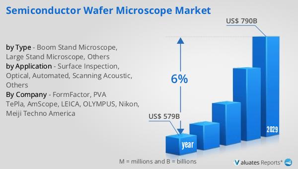
 Figure 13. Global Semiconductor Wafer Microscope Production Value (US$ Million), 2020 VS 2024 VS 2031
 Figure 14. Global Semiconductor Wafer Microscope Production Value (US$ Million) & (2020-2031)
 Figure 15. Global Semiconductor Wafer Microscope Production Capacity (Units) & (2020-2031)
 Figure 16. Global Semiconductor Wafer Microscope Production (Units) & (2020-2031)
 Figure 17. Global Semiconductor Wafer Microscope Average Price (K US$/Unit) & (2020-2031)
 Figure 18. Semiconductor Wafer Microscope Report Years Considered
 Figure 19. Semiconductor Wafer Microscope Production Share by Manufacturers in 2024
 Figure 20. Global Semiconductor Wafer Microscope Production Value Share by Manufacturers (2024)
 Figure 21. Semiconductor Wafer Microscope Market Share by Company Type (Tier 1, Tier 2, and Tier 3): 2020 VS 2024
 Figure 22. The Global 5 and 10 Largest Players: Market Share by Semiconductor Wafer Microscope Revenue in 2024
 Figure 23. Global Semiconductor Wafer Microscope Production Value by Region: 2020 VS 2024 VS 2031 (US$ Million)
 Figure 24. Global Semiconductor Wafer Microscope Production Value Market Share by Region: 2020 VS 2024 VS 2031
 Figure 25. Global Semiconductor Wafer Microscope Production Comparison by Region: 2020 VS 2024 VS 2031 (Units)
 Figure 26. Global Semiconductor Wafer Microscope Production Market Share by Region: 2020 VS 2024 VS 2031
 Figure 27. North America Semiconductor Wafer Microscope Production Value (US$ Million) Growth Rate (2020-2031)
 Figure 28. Europe Semiconductor Wafer Microscope Production Value (US$ Million) Growth Rate (2020-2031)
 Figure 29. China Semiconductor Wafer Microscope Production Value (US$ Million) Growth Rate (2020-2031)
 Figure 30. Japan Semiconductor Wafer Microscope Production Value (US$ Million) Growth Rate (2020-2031)
 Figure 31. Global Semiconductor Wafer Microscope Consumption by Region: 2020 VS 2024 VS 2031 (Units)
 Figure 32. Global Semiconductor Wafer Microscope Consumption Market Share by Region: 2020 VS 2024 VS 2031
 Figure 33. North America Semiconductor Wafer Microscope Consumption and Growth Rate (2020-2031) & (Units)
 Figure 34. North America Semiconductor Wafer Microscope Consumption Market Share by Country (2020-2031)
 Figure 35. U.S. Semiconductor Wafer Microscope Consumption and Growth Rate (2020-2031) & (Units)
 Figure 36. Canada Semiconductor Wafer Microscope Consumption and Growth Rate (2020-2031) & (Units)
 Figure 37. Europe Semiconductor Wafer Microscope Consumption and Growth Rate (2020-2031) & (Units)
 Figure 38. Europe Semiconductor Wafer Microscope Consumption Market Share by Country (2020-2031)
 Figure 39. Germany Semiconductor Wafer Microscope Consumption and Growth Rate (2020-2031) & (Units)
 Figure 40. France Semiconductor Wafer Microscope Consumption and Growth Rate (2020-2031) & (Units)
 Figure 41. U.K. Semiconductor Wafer Microscope Consumption and Growth Rate (2020-2031) & (Units)
 Figure 42. Italy Semiconductor Wafer Microscope Consumption and Growth Rate (2020-2031) & (Units)
 Figure 43. Netherlands Semiconductor Wafer Microscope Consumption and Growth Rate (2020-2031) & (Units)
 Figure 44. Asia Pacific Semiconductor Wafer Microscope Consumption and Growth Rate (2020-2031) & (Units)
 Figure 45. Asia Pacific Semiconductor Wafer Microscope Consumption Market Share by Region (2020-2031)
 Figure 46. China Semiconductor Wafer Microscope Consumption and Growth Rate (2020-2031) & (Units)
 Figure 47. Japan Semiconductor Wafer Microscope Consumption and Growth Rate (2020-2031) & (Units)
 Figure 48. South Korea Semiconductor Wafer Microscope Consumption and Growth Rate (2020-2031) & (Units)
 Figure 49. China Taiwan Semiconductor Wafer Microscope Consumption and Growth Rate (2020-2031) & (Units)
 Figure 50. Southeast Asia Semiconductor Wafer Microscope Consumption and Growth Rate (2020-2031) & (Units)
 Figure 51. India Semiconductor Wafer Microscope Consumption and Growth Rate (2020-2031) & (Units)
 Figure 52. Latin America, Middle East & Africa Semiconductor Wafer Microscope Consumption and Growth Rate (2020-2031) & (Units)
 Figure 53. Latin America, Middle East & Africa Semiconductor Wafer Microscope Consumption Market Share by Country (2020-2031)
 Figure 54. Mexico Semiconductor Wafer Microscope Consumption and Growth Rate (2020-2031) & (Units)
 Figure 55. Brazil Semiconductor Wafer Microscope Consumption and Growth Rate (2020-2031) & (Units)
 Figure 56. Turkey Semiconductor Wafer Microscope Consumption and Growth Rate (2020-2031) & (Units)
 Figure 57. GCC Countries Semiconductor Wafer Microscope Consumption and Growth Rate (2020-2031) & (Units)
 Figure 58. Global Production Market Share of Semiconductor Wafer Microscope by Type (2020-2031)
 Figure 59. Global Production Value Market Share of Semiconductor Wafer Microscope by Type (2020-2031)
 Figure 60. Global Semiconductor Wafer Microscope Price (K US$/Unit) by Type (2020-2031)
 Figure 61. Global Production Market Share of Semiconductor Wafer Microscope by Application (2020-2031)
 Figure 62. Global Production Value Market Share of Semiconductor Wafer Microscope by Application (2020-2031)
 Figure 63. Global Semiconductor Wafer Microscope Price (K US$/Unit) by Application (2020-2031)
 Figure 64. Semiconductor Wafer Microscope Value Chain
 Figure 65. Channels of Distribution (Direct Vs Distribution)
 Figure 66. Bottom-up and Top-down Approaches for This Report
 Figure 67. Data Triangulation
SELECT A FORMAT
Added to Cart
Electronic (PDF)

$2900

This license allows only one user to access the PDF.
Electronic (PDF)

$4350

This license allows 1 - 5 user to access the PDF, license is suitable for small groups of 5 users working together
Electronic (PDF)

$5800

This license allows users/teams in a same Enterprise to use this report, various departments within an enterpise can use this report
Add to Cart
Buy Now (15% Discount)

OUR CUSTOMER

SecuX Technology Inc

SIMILAR REPORTS