Wafer Fabrication Materials Market Size
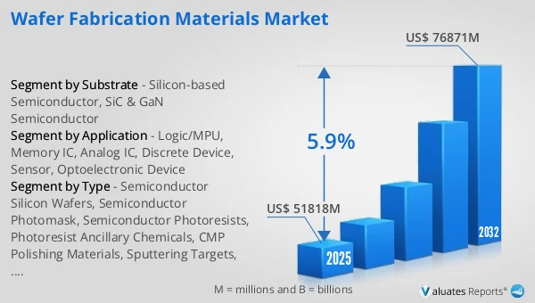
The global Wafer Fabrication Materials market was valued at US$ 51818 million in 2025 and is anticipated to reach US$ 76871 million by 2032, at a CAGR of 5.9% from 2026 to 2032.
Wafer Fabrication Materials Market
Wafer Fabrication Materials can be defined as the consumable and periodically replaced material set that enables wafer manufacturing unit processes—lithography, deposition, etch, CMP, wet clean/etch, thermal steps, and associated contamination-control infrastructure. Under your taxonomy, it spans Semiconductor Silicon Wafers, Semiconductor Photomasks, Semiconductor Photoresists and Photoresist Ancillary Chemicals (developers, primers/adhesion promoters, solvents/strippers, multilayer materials and hardmask-related chemistries), CMP Polishing Materials (slurries, pads, conditioners), Sputtering Targets, Semiconductor Gases (bulk + specialty), Wet-processing Chemicals (ultra-high-purity wet clean/etch chemicals), plus Others (e.g., filtration/purification consumables, specialty formulations and precursors, packaging and micro-environment materials). Across these categories, advanced manufacturing pushes a shared requirement set—ultra-high purity, extremely low metals/particles/organics, batch-to-batch consistency, traceability, and supply assurance—while EUV/High-NA scaling also “redefines” the material stack: leading photoresist suppliers explicitly state that EUV resists are approved for mass-production lines and continue to evolve alongside multilayer materials portfolios.
Technically and in application mapping, each material segment is tightly coupled to device architecture, node, and end-market demand. Silicon wafers are anchored by 300mm for leading-edge logic and advanced memory, while 200mm-and-below retain structural relevance for power/analog and specialty nodes; SEMI reports that worldwide silicon wafer shipments improved year-on-year in Q3 2025 and highlights that 300mm shipment growth was fueled by AI-related demand for advanced logic, cloud computing, and memory. Photomasks face rising complexity as the ecosystem moves toward 2nm and High-NA EUV, with top mask suppliers publicly entering joint R&D for EUV and High-NA mask capabilities. Photoresists and ancillary chemicals increasingly extend beyond “main resist” to multilayer materials/hardmask-related stacks and process-support chemistries (JSR describes a portfolio spanning i-line to EUV resists and multilayer materials). CMP consumables scale with layer counts and new materials; Entegris positions its CMP slurry solutions for polishing ultra-hard materials including SiC and GaN, while industry commentary indicates pad supply is highly concentrated. Sputtering targets remain essential PVD consumables where high purity and low particle generation are decisive (JX Advanced Metals details high-purity, low-particle semiconductor sputtering targets and applications). For gases and wet chemicals, quality and cost are co-defined by supply mode plus purification/distribution infrastructure; Air Liquide states it supplies gases by cylinder, bulk, pipeline, or on-site generation, and Reuters reports Air Liquide’s dedicated investment to supply ultra-pure nitrogen and other gases to Micron—illustrating the “materials infrastructure” coupling to leading-edge capacity expansion.
Competitively, wafer-fab materials exhibit a “high concentration by segment + accelerating localization/second-sourcing in selected segments” pattern, driven by qualification barriers and supply-chain resilience priorities. Silicon wafers, advanced photomasks, advanced resists, CMP critical consumables, specialty gases, and ultra-high-purity wet chemicals typically require long qualification cycles and therefore skew toward incumbent leaders; meanwhile, localization is visible in capacity investments. Reuters reports that GlobalWafers is preparing a phase-two expansion at its Texas 300mm wafer plant (the first fully integrated advanced 300mm wafer facility built in the U.S. in more than two decades), citing growing customer demand—an example of advanced manufacturing regionalization pulling upstream material ecosystems onshore. Photomask capability upgrades for 2nm/High-NA EUV further raise entry barriers and intensify OEM–mask shop–fab ecosystem coupling. Forward trends/drivers can be summarized as: AI/HPC and HBM-led capacity build-outs that lift consumption and specification levels across wafers, EUV-related masks/resists, CMP, and gases/chemicals ; increasing lithography complexity (EUV/High-NA and multi-patterning) that expands multilayer/ancillary chemistry requirements and defect-control demands ; and regulatory/safety plus sustainability constraints (hazmat logistics, purity assurance, waste handling) reinforcing investments in on-site supply models and localized, resilient supply chains.
This report delivers a comprehensive overview of the global Wafer Fabrication Materials market, with both quantitative and qualitative analyses, to help readers develop growth strategies, assess the competitive landscape, evaluate their position in the current market, and make informed business decisions regarding Wafer Fabrication Materials. The Wafer Fabrication Materials market size, estimates, and forecasts are provided in terms of revenue (US$ millions), with 2025 as the base year and historical and forecast data for 2021–2032.
The report segments the global Wafer Fabrication Materials market comprehensively. Regional market sizes by Type, by Application, by Wafer Size, and by player are also provided. For deeper insight, the report profiles the competitive landscape, key competitors, and their respective market rankings, and discusses technological trends and new product developments.
This report will assist Wafer Fabrication Materials manufacturers, new entrants, and companies across the industry value chain with information on revenues, sales volume, and average prices for the overall market and its sub-segments, by company, by Type, by Application, and by region.
Market Segmentation
Scope of Wafer Fabrication Materials Market Report
| Report Metric |
Details |
| Report Name |
Wafer Fabrication Materials Market |
| Accounted market size in 2025 |
US$ 51818 million |
| Forecasted market size in 2032 |
US$ 76871 million |
| CAGR |
5.9% |
| Base Year |
2025 |
| Forecasted years |
2026 - 2032 |
| Segment by Type |
- Semiconductor Silicon Wafers
- Semiconductor Photomask
- Semiconductor Photoresists
- Photoresist Ancillary Chemicals
- CMP Polishing Materials
- Sputtering Targets
- Semiconductor Gases
- Wet-processing Chemicals
- Others
|
| Segment by Wafer Size |
- 300mm Wafer Fab
- 200mm Wafer Fab
- Other Size
|
| Segment by Substrate |
- Silicon-based Semiconductor
- SiC & GaN Semiconductor
|
| Segment by Application |
- Logic/MPU
- Memory IC
- Analog IC
- Discrete Device
- Sensor
- Optoelectronic Device
|
| By Region |
- North America (United States, Canada)
- Europe (Germany, France, UK, Italy, Russia) Rest of Europe
- Nordic Countries
- Asia-Pacific (China, Japan, South Korea)
- Southeast Asia (India, Australia)
- Rest of Asia
- Latin America (Mexico, Brazil)
- Rest of Latin America
- Middle East & Africa (Turkey, Saudi Arabia, UAE, Rest of MEA)
|
| By Company |
Shin-Etsu Chemical, SUMCO, GlobalWafers, Siltronic AG, SK Siltron, FST Corporation, Wafer Works Corporation, National Silicon Industry Group (NSIG), Zhonghuan Advanced Semiconductor Materials, Hangzhou Lion Microelectronics, Hangzhou Semiconductor Wafer, GRINM Semiconductor Materials, Shanghai Advanced Silicon Technology (AST), Xi'an ESWIN Material Technology, Soitec, TOKYO OHKA KOGYO CO., LTD. (TOK), JSR, Qnity, Fujifilm, Sumitomo Chemical, Dongjin Semichem, Merck KGaA (AZ), Photronics, Toppan, DNP, Hoya, SK-Electronics, LG Innotek, ShenZheng QingVi, Taiwan Mask, Nippon Filcon, Compugraphics, Newway Photomask, Resonac, Fujimi Incorporated, AGC, KC Tech, Anjimirco Shanghai, Soulbrain, Hubei Dinglong, JX Advanced Metals, Materion, Konfoong Materials International, Linde, Proterial, Plansee SE, TOSOH, Honeywell, Air Liquide, Solvay, Air Products, Kanto Denka Kogyo, BASF, Kanto Chemical, Chang Chun Group, Tama Chemicals |
| Forecast units |
USD million in value |
| Report coverage |
Revenue and volume forecast, company share, competitive landscape, growth factors and trends |
Chapter Outline
- Chapter 1: Defines the scope of the report and presents an executive summary of market segments (by Type, by Application, by Wafer Size, etc.), including the size of each segment and its future growth potential. It offers a high-level view of the current market and its likely evolution in the short, medium, and long term.
- Chapter 2: Summarizes global and regional market size and outlines market dynamics and recent developments, including key drivers, restraints, challenges and risks for industry participants, and relevant policy analysis.
- Chapter 3: Provides a detailed view of the competitive landscape for Wafer Fabrication Materials companies, covering revenue share, development plans, and mergers and acquisitions.
- Chapter 4: Analyzes segments by Type, detailing the size and growth potential of each segment to help readers identify blue-ocean opportunities.
- Chapter 5: Analyzes segments by Application, detailing the size and growth potential of each downstream segment to help readers identify blue-ocean opportunities.
- Chapter 6–10: Regional deep dives (North America, Europe, Asia Pacific, Latin America, Middle East & Africa) broken down by country. Each chapter quantifies market size and growth potential by region and key countries, and outlines market development, outlook, addressable space, and capacity.
- Chapter 11: Profiles key players, presenting essential information on leading companies, including product/ service offerings, revenue, gross margin, product introductions/portfolios, recent developments, etc.
- Chapter 12: Key findings and conclusions of the report.
FAQ for this report
How fast is Wafer Fabrication Materials Market growing?
Ans: The Wafer Fabrication Materials Market witnessing a CAGR of 5.9% during the forecast period 2026-2032.
What is the Wafer Fabrication Materials Market size in 2032?
Ans: The Wafer Fabrication Materials Market size in 2032 will be US$ 76871 million.
Who are the main players in the Wafer Fabrication Materials Market report?
Ans: The main players in the Wafer Fabrication Materials Market are Shin-Etsu Chemical, SUMCO, GlobalWafers, Siltronic AG, SK Siltron, FST Corporation, Wafer Works Corporation, National Silicon Industry Group (NSIG), Zhonghuan Advanced Semiconductor Materials, Hangzhou Lion Microelectronics, Hangzhou Semiconductor Wafer, GRINM Semiconductor Materials, Shanghai Advanced Silicon Technology (AST), Xi'an ESWIN Material Technology, Soitec, TOKYO OHKA KOGYO CO., LTD. (TOK), JSR, Qnity, Fujifilm, Sumitomo Chemical, Dongjin Semichem, Merck KGaA (AZ), Photronics, Toppan, DNP, Hoya, SK-Electronics, LG Innotek, ShenZheng QingVi, Taiwan Mask, Nippon Filcon, Compugraphics, Newway Photomask, Resonac, Fujimi Incorporated, AGC, KC Tech, Anjimirco Shanghai, Soulbrain, Hubei Dinglong, JX Advanced Metals, Materion, Konfoong Materials International, Linde, Proterial, Plansee SE, TOSOH, Honeywell, Air Liquide, Solvay, Air Products, Kanto Denka Kogyo, BASF, Kanto Chemical, Chang Chun Group, Tama Chemicals
What are the Application segmentation covered in the Wafer Fabrication Materials Market report?
Ans: The Applications covered in the Wafer Fabrication Materials Market report are Logic/MPU, Memory IC, Analog IC, Discrete Device, Sensor, Optoelectronic Device
What are the Type segmentation covered in the Wafer Fabrication Materials Market report?
Ans: The Types covered in the Wafer Fabrication Materials Market report are Semiconductor Silicon Wafers, Semiconductor Photomask, Semiconductor Photoresists, Photoresist Ancillary Chemicals, CMP Polishing Materials, Sputtering Targets, Semiconductor Gases, Wet-processing Chemicals, Others