FEATURED COMPANIES
ics
Kawasaki
Kensington Laboratories
Wafer Handling Equipment Market Size
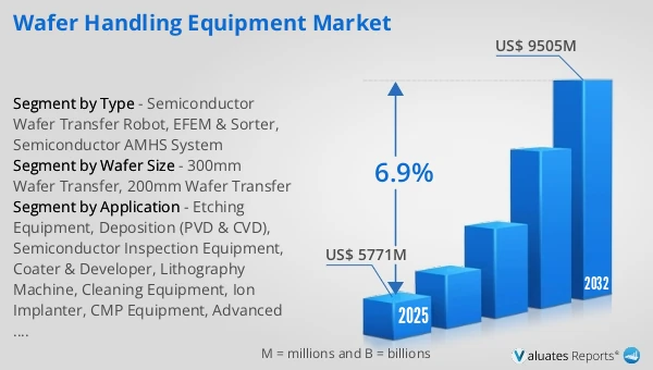
The global Wafer Handling Equipment market was valued at US$ 5771 million in 2025 and is anticipated to reach US$ 9505 million by 2032, at a CAGR of 6.9% from 2026 to 2032.
Wafer Handling Equipment Market
Wafer Handling Equipment generally refers to the automation hardware stack that enables carrier (FOUP/FOSB/cassette) and wafer transfer, positioning, buffering, and exchange between factory logistics and process tools, as well as within multi-module tools. In practical industry scope, it is convenient to view it in three layers: (1) Factory-level AMHS (Automated Material Handling System) for in-fab storage and transport—SEMI E87 defines AMHS as “an automated system to store and transport materials within the factory” and defines a load port as “the interface location on the equipment where carriers are loaded and unloaded”; typical physical implementations include OHT/overhead transport, stockers/automated storage, and buffer stations. (2) Tool front-end / factory interface, where EFEM (Equipment Front-End Module) acts as the standardized interface between carrier transport and the process tool; a Brooks Jet EFEM manual describes the system as “the link between the factory’s Material Transport System and the Process Tool,” integrating load ports, an atmospheric robot, an aligner, and a mini-environment/FFU on an integrated frame. (3) In-tool transfer, dominated by atmospheric and vacuum wafer transfer robots / wafer transfer modules inside cluster tools, moving wafers among load locks, process chambers, and internal buffers. In addition, wafer sorters/handlers are widely used as wafer-flow infrastructure (reordering, splitting/merging, and transferring wafers between carriers and stations) and are often included when the “wafer handling” scope is defined from a fab operations standpoint.
From a product and technology decomposition standpoint, EFEM/sorter-class equipment is typically modular and built from: SEMI-standard load ports and docking/FOUP opening mechanisms, wafer transfer robots (single/dual end-effector, direct-drive servo, continuous rotation), pre-alignment/alignment modules (notch/flat detection and centering), mapping/slot scanning, wafer ID/OCR, internal buffers/exchange slots, mini-environment plus fan/filter unit (FFU), and safety interlocks with factory communications (SECS/GEM and commonly referenced carrier handoff/tracking standards such as E84/E87/E90). Public EFEM descriptions explicitly link adoption to yield/throughput and contamination control: Fala characterizes an EFEM as the “mainstay of semiconductor automation” moving wafers between ultra-clean carriers and processing/metrology/test systems, noting that shrinking geometries make previously tolerable contamination levels unacceptable and that automation reduces operator-related contamination. For sorters, an InnoLas brochure describes wafer sorting systems that can sort/split/merge/transfer wafers by ID/thickness/weight, with options such as edge-grip handling for backside cleanliness, Class 1 mini-environments, and compatibility with AGV/OHT integration; it also notes that such sorting platforms can be used “as a so called EFEM” (a clean transfer module for loading/unloading another tool). On the vacuum side, Brooks highlights vacuum robots transferring wafers between process modules in cluster tools and emphasizes large installed bases at major fabs/tool OEMs—reflecting the centrality of vacuum handling to modern etch/deposition cluster architectures.
In applications and value chain terms, wafer handling equipment underpins virtually all fab operations: tool loading/unloading for deposition/etch/clean/CMP, metrology/inspection routing, and post-process logistics such as lot splitting/merging and reordering prior to downstream steps. Standardized interfaces are a core enabler of scalable automation: SEMI E15.1 states that 300 mm load-port dimensional requirements are intended to promote a uniform equipment–factory physical interface and facilitate automated wafer carrier transport systems (with SEMI E15 covering smaller wafers). At the factory scale, automation leaders describe highly automated 300 mm fabs with long interbay tracks, large fleets of wafer transport vehicles operating 24/7, overhead transport systems, and nitrogen-purged storage for clean handling and storage continuity. Upstream supply includes precision motion/control components (servo motors/drives, reducers/transmissions, encoders, linear guides/bearings), clean/vacuum modules (seals, vacuum components, FFU/filters, ESD/ionization), sensing/vision (mapping, OCR, alignment sensors), and factory-control software; midstream comprises robot/EFEM/sorter/AMHS OEMs and system integrators; downstream includes tool OEMs and fab operators. Key industry trends and drivers are: (i) higher automation density driven by fab expansions and more complex routing; (ii) tighter contamination/yield requirements (greater mini-environment penetration and backside-clean handling such as edge-grip); (iii) stronger standardization and interoperability demands (load-port and carrier-management interfaces enabling modular integration); and (iv) “lights-out” productivity goals (higher throughput, lower MTTR, and more diagnostics/predictive maintenance capability).
This report delivers a comprehensive overview of the global Wafer Handling Equipment market, with both quantitative and qualitative analyses, to help readers develop growth strategies, assess the competitive landscape, evaluate their position in the current market, and make informed business decisions regarding Wafer Handling Equipment. The Wafer Handling Equipment market size, estimates, and forecasts are provided in terms of revenue (US$ millions), with 2025 as the base year and historical and forecast data for 2021–2032.
The report segments the global Wafer Handling Equipment market comprehensively. Regional market sizes by Type, by Wafer Size, by Application, and by player are also provided. For deeper insight, the report profiles the competitive landscape, key competitors, and their respective market rankings, and discusses technological trends and new product developments.
This report will assist Wafer Handling Equipment manufacturers, new entrants, and companies across the industry value chain with information on revenues, sales volume, and average prices for the overall market and its sub-segments, by company, by Type, by Wafer Size, and by region.
Market Segmentation
Scope of Wafer Handling Equipment Market Report
| Report Metric |
Details |
| Report Name |
Wafer Handling Equipment Market |
| Accounted market size in 2025 |
US$ 5771 million |
| Forecasted market size in 2032 |
US$ 9505 million |
| CAGR |
6.9% |
| Base Year |
2025 |
| Forecasted years |
2026 - 2032 |
| Segment by Type |
- Semiconductor Wafer Transfer Robot
- EFEM & Sorter
- Semiconductor AMHS System
|
| Segment by Application |
- Etching Equipment
- Deposition (PVD & CVD)
- Semiconductor Inspection Equipment
- Coater & Developer
- Lithography Machine
- Cleaning Equipment
- Ion Implanter
- CMP Equipment
- Advanced Packaging
- Others
|
| Segment by Wafer Size |
- 300mm Wafer Transfer
- 200mm Wafer Transfer
|
| By Region |
- North America (United States, Canada)
- Europe (Germany, France, UK, Italy, Russia) Rest of Europe
- Nordic Countries
- Asia-Pacific (China, Japan, South Korea)
- Southeast Asia (India, Australia)
- Rest of Asia
- Latin America (Mexico, Brazil)
- Rest of Latin America
- Middle East & Africa (Turkey, Saudi Arabia, UAE, Rest of MEA)
|
| By Company |
Kawasaki Robotics, RORZE Corporation, Brooks Automation, DAIHEN Corporation, Hirata Corporation, Yaskawa, Nidec (Genmark Automation), JEL Corporation, Robostar, Robots and Design (RND), HYULIM Robot, RAONTEC Inc, Cymechs Inc, Sumitomo Heavy Industries (SHI), Tazmo, Rexxam Co Ltd, ULVAC, Kensington Laboratories, EPSON Robots, Hine Automation, Moog Inc, Innovative Robotics, Stäubli, Sinfonia Technology, Murata Machinery, Daifuku, SFA Engineering Corporation, SEMES, SYNUS Tech (Suzhou Nsynu Semiconductor Equipment), Mirle Automation, SMCore, Shinsung E&G Co., Ltd, SEMI Total Solution Inc, Stratus Automation, Fabmatics, MFSG, Kenmec Mechanical Engineering, Shanghai Guona Semiconductor, isel Germany AG, Sanwa Engineering Corporation, Siasun Robot & Automation, HIWIN Corporation, He-Five LLC., Shibaura Machine, Shanghai Future Technology, PHT Inc., Wuxi Xinghui Technology, HongHu (Suzhou) Semiconductor Technology, Shanghai Fortrend Technology, Shanghai MICSON Industrial Automation, MeetFuture Technology (Shanghai) |
| Forecast units |
USD million in value |
| Report coverage |
Revenue and volume forecast, company share, competitive landscape, growth factors and trends |
Chapter Outline
- Chapter 1: Defines the scope of the report and presents an executive summary of market segments (by Type, by Wafer Size, by Application, etc.), including the size of each segment and its future growth potential. It offers a high-level view of the current market and its likely evolution in the short, medium, and long term.
- Chapter 2: Summarizes global and regional market size and outlines market dynamics and recent developments, including key drivers, restraints, challenges and risks for industry participants, and relevant policy analysis.
- Chapter 3: Provides a detailed view of the competitive landscape for Wafer Handling Equipment companies, covering revenue share, development plans, and mergers and acquisitions.
- Chapter 4: Analyzes segments by Type, detailing the size and growth potential of each segment to help readers identify blue-ocean opportunities.
- Chapter 5: Analyzes segments by Wafer Size, detailing the size and growth potential of each downstream segment to help readers identify blue-ocean opportunities.
- Chapter 6–10: Regional deep dives (North America, Europe, Asia Pacific, Latin America, Middle East & Africa) broken down by country. Each chapter quantifies market size and growth potential by region and key countries, and outlines market development, outlook, addressable space, and capacity.
- Chapter 11: Profiles key players, presenting essential information on leading companies, including product/ service offerings, revenue, gross margin, product introductions/portfolios, recent developments, etc.
- Chapter 12: Key findings and conclusions of the report.
FAQ for this report
How fast is Wafer Handling Equipment Market growing?
Ans: The Wafer Handling Equipment Market witnessing a CAGR of 6.9% during the forecast period 2026-2032.
What is the Wafer Handling Equipment Market size in 2032?
Ans: The Wafer Handling Equipment Market size in 2032 will be US$ 9505 million.
Who are the main players in the Wafer Handling Equipment Market report?
Ans: The main players in the Wafer Handling Equipment Market are Kawasaki Robotics, RORZE Corporation, Brooks Automation, DAIHEN Corporation, Hirata Corporation, Yaskawa, Nidec (Genmark Automation), JEL Corporation, Robostar, Robots and Design (RND), HYULIM Robot, RAONTEC Inc, Cymechs Inc, Sumitomo Heavy Industries (SHI), Tazmo, Rexxam Co Ltd, ULVAC, Kensington Laboratories, EPSON Robots, Hine Automation, Moog Inc, Innovative Robotics, Stäubli, Sinfonia Technology, Murata Machinery, Daifuku, SFA Engineering Corporation, SEMES, SYNUS Tech (Suzhou Nsynu Semiconductor Equipment), Mirle Automation, SMCore, Shinsung E&G Co., Ltd, SEMI Total Solution Inc, Stratus Automation, Fabmatics, MFSG, Kenmec Mechanical Engineering, Shanghai Guona Semiconductor, isel Germany AG, Sanwa Engineering Corporation, Siasun Robot & Automation, HIWIN Corporation, He-Five LLC., Shibaura Machine, Shanghai Future Technology, PHT Inc., Wuxi Xinghui Technology, HongHu (Suzhou) Semiconductor Technology, Shanghai Fortrend Technology, Shanghai MICSON Industrial Automation, MeetFuture Technology (Shanghai)
What are the Application segmentation covered in the Wafer Handling Equipment Market report?
Ans: The Applications covered in the Wafer Handling Equipment Market report are Etching Equipment, Deposition (PVD & CVD), Semiconductor Inspection Equipment, Coater & Developer, Lithography Machine, Cleaning Equipment, Ion Implanter, CMP Equipment, Advanced Packaging, Others
What are the Type segmentation covered in the Wafer Handling Equipment Market report?
Ans: The Types covered in the Wafer Handling Equipment Market report are Semiconductor Wafer Transfer Robot, EFEM & Sorter, Semiconductor AMHS System