List of Tables
Table 1. Global Semiconductor Wafer Defect Inspection System Market Value by Type (US$ Million), 2025 vs 2032
Table 2. Global Semiconductor Wafer Defect Inspection System Market Value by Application (US$ Million), 2025 vs 2032
Table 3. Global Semiconductor Wafer Defect Inspection System Production Capacity (Units) by Manufacturers in 2025
Table 4. Global Semiconductor Wafer Defect Inspection System Production by Manufacturers (Units), 2021–2026
Table 5. Global Semiconductor Wafer Defect Inspection System Production Market Share by Manufacturers (2021–2026)
Table 6. Global Semiconductor Wafer Defect Inspection System Production Value by Manufacturers (US$ Million), 2021–2026
Table 7. Global Semiconductor Wafer Defect Inspection System Production Value Share by Manufacturers (2021–2026)
Table 8. Global Key Players of Semiconductor Wafer Defect Inspection System, Industry Ranking, 2024 vs 2025
Table 9. Classification of Companies by Tier (Tier 1, Tier 2, Tier 3), based on Semiconductor Wafer Defect Inspection System Production Value, 2025
Table 10. Global Market Semiconductor Wafer Defect Inspection System Average Price by Manufacturers (US$/Unit), 2021–2026
Table 11. Global Key Manufacturers of Semiconductor Wafer Defect Inspection System, Manufacturing Footprints and Headquarters
Table 12. Global Key Manufacturers of Semiconductor Wafer Defect Inspection System, Product Offerings and Applications
Table 13. Global Key Manufacturers of Semiconductor Wafer Defect Inspection System, Date of Entry into the Industry
Table 14. Global Semiconductor Wafer Defect Inspection System Manufacturers Market Concentration Ratio (CR5 and HHI)
Table 15. Mergers & Acquisitions and Expansion Plans
Table 16. Global Semiconductor Wafer Defect Inspection System Production Value by Region: 2021 vs 2025 vs 2032 (US$ Million)
Table 17. Global Semiconductor Wafer Defect Inspection System Production Value (US$ Million) by Region (2021–2026)
Table 18. Global Semiconductor Wafer Defect Inspection System Production Value Market Share by Region (2021–2026)
Table 19. Global Semiconductor Wafer Defect Inspection System Production Value (US$ Million) Forecast by Region (2027–2032)
Table 20. Global Semiconductor Wafer Defect Inspection System Production Value Market Share Forecast by Region (2027–2032)
Table 21. Global Semiconductor Wafer Defect Inspection System Production Comparison by Region: 2021 vs 2025 vs 2032 (Units)
Table 22. Global Semiconductor Wafer Defect Inspection System Production (Units) by Region (2021–2026)
Table 23. Global Semiconductor Wafer Defect Inspection System Production Market Share by Region (2021–2026)
Table 24. Global Semiconductor Wafer Defect Inspection System Production (Units) Forecast by Region (2027–2032)
Table 25. Global Semiconductor Wafer Defect Inspection System Production Market Share Forecast by Region (2027–2032)
Table 26. Global Semiconductor Wafer Defect Inspection System Market Average Price (US$/Unit) by Region (2021–2026)
Table 27. Global Semiconductor Wafer Defect Inspection System Market Average Price (US$/Unit) by Region (2027–2032)
Table 28. Global Semiconductor Wafer Defect Inspection System Consumption Growth Rate by Region: 2021 vs 2025 vs 2032 (Units)
Table 29. Global Semiconductor Wafer Defect Inspection System Consumption by Region (Units), 2021–2026
Table 30. Global Semiconductor Wafer Defect Inspection System Consumption Market Share by Region (2021–2026)
Table 31. Global Semiconductor Wafer Defect Inspection System Forecasted Consumption by Region (Units), 2027–2032
Table 32. Global Semiconductor Wafer Defect Inspection System Forecasted Consumption Market Share by Region (2027–2032)
Table 33. North America Semiconductor Wafer Defect Inspection System Consumption Growth Rate by Country: 2021 vs 2025 vs 2032 (Units)
Table 34. North America Semiconductor Wafer Defect Inspection System Consumption by Country (Units), 2021–2026
Table 35. North America Semiconductor Wafer Defect Inspection System Consumption by Country (Units), 2027–2032
Table 36. Europe Semiconductor Wafer Defect Inspection System Consumption Growth Rate by Country: 2021 vs 2025 vs 2032 (Units)
Table 37. Europe Semiconductor Wafer Defect Inspection System Consumption by Country (Units), 2021–2026
Table 38. Europe Semiconductor Wafer Defect Inspection System Consumption by Country (Units), 2027–2032
Table 39. Asia Pacific Semiconductor Wafer Defect Inspection System Consumption Growth Rate by Region: 2021 vs 2025 vs 2032 (Units)
Table 40. Asia Pacific Semiconductor Wafer Defect Inspection System Consumption by Region (Units), 2021–2026
Table 41. Asia Pacific Semiconductor Wafer Defect Inspection System Consumption by Region (Units), 2027–2032
Table 42. Latin America, Middle East & Africa Semiconductor Wafer Defect Inspection System Consumption Growth Rate by Country: 2021 vs 2025 vs 2032 (Units)
Table 43. Latin America, Middle East & Africa Semiconductor Wafer Defect Inspection System Consumption by Country (Units), 2021–2026
Table 44. Latin America, Middle East & Africa Semiconductor Wafer Defect Inspection System Consumption by Country (Units), 2027–2032
Table 45. Global Semiconductor Wafer Defect Inspection System Production (Units) by Type (2021–2026)
Table 46. Global Semiconductor Wafer Defect Inspection System Production (Units) by Type (2027–2032)
Table 47. Global Semiconductor Wafer Defect Inspection System Production Market Share by Type (2021–2026)
Table 48. Global Semiconductor Wafer Defect Inspection System Production Market Share by Type (2027–2032)
Table 49. Global Semiconductor Wafer Defect Inspection System Production Value (US$ Million) by Type (2021–2026)
Table 50. Global Semiconductor Wafer Defect Inspection System Production Value (US$ Million) by Type (2027–2032)
Table 51. Global Semiconductor Wafer Defect Inspection System Production Value Market Share by Type (2021–2026)
Table 52. Global Semiconductor Wafer Defect Inspection System Production Value Market Share by Type (2027–2032)
Table 53. Global Semiconductor Wafer Defect Inspection System Price (US$/Unit) by Type (2021–2026)
Table 54. Global Semiconductor Wafer Defect Inspection System Price (US$/Unit) by Type (2027–2032)
Table 55. Global Semiconductor Wafer Defect Inspection System Production (Units) by Application (2021–2026)
Table 56. Global Semiconductor Wafer Defect Inspection System Production (Units) by Application (2027–2032)
Table 57. Global Semiconductor Wafer Defect Inspection System Production Market Share by Application (2021–2026)
Table 58. Global Semiconductor Wafer Defect Inspection System Production Market Share by Application (2027–2032)
Table 59. Global Semiconductor Wafer Defect Inspection System Production Value (US$ Million) by Application (2021–2026)
Table 60. Global Semiconductor Wafer Defect Inspection System Production Value (US$ Million) by Application (2027–2032)
Table 61. Global Semiconductor Wafer Defect Inspection System Production Value Market Share by Application (2021–2026)
Table 62. Global Semiconductor Wafer Defect Inspection System Production Value Market Share by Application (2027–2032)
Table 63. Global Semiconductor Wafer Defect Inspection System Price (US$/Unit) by Application (2021–2026)
Table 64. Global Semiconductor Wafer Defect Inspection System Price (US$/Unit) by Application (2027–2032)
Table 65. KLA Corporation Semiconductor Wafer Defect Inspection System Company Information
Table 66. KLA Corporation Semiconductor Wafer Defect Inspection System Specification and Application
Table 67. KLA Corporation Semiconductor Wafer Defect Inspection System Production (Units), Value (US$ Million), Price (US$/Unit) and Gross Margin (2021–2026)
Table 68. KLA Corporation Main Business and Markets Served
Table 69. KLA Corporation Recent Developments/Updates
Table 70. Applied Materials Semiconductor Wafer Defect Inspection System Company Information
Table 71. Applied Materials Semiconductor Wafer Defect Inspection System Specification and Application
Table 72. Applied Materials Semiconductor Wafer Defect Inspection System Production (Units), Value (US$ Million), Price (US$/Unit) and Gross Margin (2021–2026)
Table 73. Applied Materials Main Business and Markets Served
Table 74. Applied Materials Recent Developments/Updates
Table 75. Lasertec Semiconductor Wafer Defect Inspection System Company Information
Table 76. Lasertec Semiconductor Wafer Defect Inspection System Specification and Application
Table 77. Lasertec Semiconductor Wafer Defect Inspection System Production (Units), Value (US$ Million), Price (US$/Unit) and Gross Margin (2021–2026)
Table 78. Lasertec Main Business and Markets Served
Table 79. Lasertec Recent Developments/Updates
Table 80. Hitachi High-Tech Corporation Semiconductor Wafer Defect Inspection System Company Information
Table 81. Hitachi High-Tech Corporation Semiconductor Wafer Defect Inspection System Specification and Application
Table 82. Hitachi High-Tech Corporation Semiconductor Wafer Defect Inspection System Production (Units), Value (US$ Million), Price (US$/Unit) and Gross Margin (2021–2026)
Table 83. Hitachi High-Tech Corporation Main Business and Markets Served
Table 84. Hitachi High-Tech Corporation Recent Developments/Updates
Table 85. ASML Semiconductor Wafer Defect Inspection System Company Information
Table 86. ASML Semiconductor Wafer Defect Inspection System Specification and Application
Table 87. ASML Semiconductor Wafer Defect Inspection System Production (Units), Value (US$ Million), Price (US$/Unit) and Gross Margin (2021–2026)
Table 88. ASML Main Business and Markets Served
Table 89. ASML Recent Developments/Updates
Table 90. Onto Innovation Semiconductor Wafer Defect Inspection System Company Information
Table 91. Onto Innovation Semiconductor Wafer Defect Inspection System Specification and Application
Table 92. Onto Innovation Semiconductor Wafer Defect Inspection System Production (Units), Value (US$ Million), Price (US$/Unit) and Gross Margin (2021–2026)
Table 93. Onto Innovation Main Business and Markets Served
Table 94. Onto Innovation Recent Developments/Updates
Table 95. Camtek Semiconductor Wafer Defect Inspection System Company Information
Table 96. Camtek Semiconductor Wafer Defect Inspection System Specification and Application
Table 97. Camtek Semiconductor Wafer Defect Inspection System Production (Units), Value (US$ Million), Price (US$/Unit) and Gross Margin (2021–2026)
Table 98. Camtek Main Business and Markets Served
Table 99. Camtek Recent Developments/Updates
Table 100. SCREEN Semiconductor Solutions Semiconductor Wafer Defect Inspection System Company Information
Table 101. SCREEN Semiconductor Solutions Semiconductor Wafer Defect Inspection System Specification and Application
Table 102. SCREEN Semiconductor Solutions Semiconductor Wafer Defect Inspection System Production (Units), Value (US$ Million), Price (US$/Unit) and Gross Margin (2021–2026)
Table 103. SCREEN Semiconductor Solutions Main Business and Markets Served
Table 104. SCREEN Semiconductor Solutions Recent Developments/Updates
Table 105. Skyverse Technology Semiconductor Wafer Defect Inspection System Company Information
Table 106. Skyverse Technology Semiconductor Wafer Defect Inspection System Specification and Application
Table 107. Skyverse Technology Semiconductor Wafer Defect Inspection System Production (Units), Value (US$ Million), Price (US$/Unit) and Gross Margin (2021–2026)
Table 108. Skyverse Technology Main Business and Markets Served
Table 109. Skyverse Technology Recent Developments/Updates
Table 110. Toray Engineering Semiconductor Wafer Defect Inspection System Company Information
Table 111. Toray Engineering Semiconductor Wafer Defect Inspection System Specification and Application
Table 112. Toray Engineering Semiconductor Wafer Defect Inspection System Production (Units), Value (US$ Million), Price (US$/Unit) and Gross Margin (2021–2026)
Table 113. Toray Engineering Main Business and Markets Served
Table 114. Toray Engineering Recent Developments/Updates
Table 115. NEXTIN Semiconductor Wafer Defect Inspection System Company Information
Table 116. NEXTIN Semiconductor Wafer Defect Inspection System Specification and Application
Table 117. NEXTIN Semiconductor Wafer Defect Inspection System Production (Units), Value (US$ Million), Price (US$/Unit) and Gross Margin (2021–2026)
Table 118. NEXTIN Main Business and Markets Served
Table 119. NEXTIN Recent Developments/Updates
Table 120. Suzhou TZTEK (Muetec) Semiconductor Wafer Defect Inspection System Company Information
Table 121. Suzhou TZTEK (Muetec) Semiconductor Wafer Defect Inspection System Specification and Application
Table 122. Suzhou TZTEK (Muetec) Semiconductor Wafer Defect Inspection System Production (Units), Value (US$ Million), Price (US$/Unit) and Gross Margin (2021–2026)
Table 123. Suzhou TZTEK (Muetec) Main Business and Markets Served
Table 124. Suzhou TZTEK (Muetec) Recent Developments/Updates
Table 125. Microtronic Semiconductor Wafer Defect Inspection System Company Information
Table 126. Microtronic Semiconductor Wafer Defect Inspection System Specification and Application
Table 127. Microtronic Semiconductor Wafer Defect Inspection System Production (Units), Value (US$ Million), Price (US$/Unit) and Gross Margin (2021–2026)
Table 128. Microtronic Main Business and Markets Served
Table 129. Microtronic Recent Developments/Updates
Table 130. Bruker Semiconductor Wafer Defect Inspection System Company Information
Table 131. Bruker Semiconductor Wafer Defect Inspection System Specification and Application
Table 132. Bruker Semiconductor Wafer Defect Inspection System Production (Units), Value (US$ Million), Price (US$/Unit) and Gross Margin (2021–2026)
Table 133. Bruker Main Business and Markets Served
Table 134. Bruker Recent Developments/Updates
Table 135. SMEE Semiconductor Wafer Defect Inspection System Company Information
Table 136. SMEE Semiconductor Wafer Defect Inspection System Specification and Application
Table 137. SMEE Semiconductor Wafer Defect Inspection System Production (Units), Value (US$ Million), Price (US$/Unit) and Gross Margin (2021–2026)
Table 138. SMEE Main Business and Markets Served
Table 139. SMEE Recent Developments/Updates
Table 140. Hangzhou Changchuan Technology Semiconductor Wafer Defect Inspection System Company Information
Table 141. Hangzhou Changchuan Technology Semiconductor Wafer Defect Inspection System Specification and Application
Table 142. Hangzhou Changchuan Technology Semiconductor Wafer Defect Inspection System Production (Units), Value (US$ Million), Price (US$/Unit) and Gross Margin (2021–2026)
Table 143. Hangzhou Changchuan Technology Main Business and Markets Served
Table 144. Hangzhou Changchuan Technology Recent Developments/Updates
Table 145. Wuhan Jingce Electronic Group Semiconductor Wafer Defect Inspection System Company Information
Table 146. Wuhan Jingce Electronic Group Semiconductor Wafer Defect Inspection System Specification and Application
Table 147. Wuhan Jingce Electronic Group Semiconductor Wafer Defect Inspection System Production (Units), Value (US$ Million), Price (US$/Unit) and Gross Margin (2021–2026)
Table 148. Wuhan Jingce Electronic Group Main Business and Markets Served
Table 149. Wuhan Jingce Electronic Group Recent Developments/Updates
Table 150. Angkun Vision (Beijing) Technology Semiconductor Wafer Defect Inspection System Company Information
Table 151. Angkun Vision (Beijing) Technology Semiconductor Wafer Defect Inspection System Specification and Application
Table 152. Angkun Vision (Beijing) Technology Semiconductor Wafer Defect Inspection System Production (Units), Value (US$ Million), Price (US$/Unit) and Gross Margin (2021–2026)
Table 153. Angkun Vision (Beijing) Technology Main Business and Markets Served
Table 154. Angkun Vision (Beijing) Technology Recent Developments/Updates
Table 155. Nanotronics Semiconductor Wafer Defect Inspection System Company Information
Table 156. Nanotronics Semiconductor Wafer Defect Inspection System Specification and Application
Table 157. Nanotronics Semiconductor Wafer Defect Inspection System Production (Units), Value (US$ Million), Price (US$/Unit) and Gross Margin (2021–2026)
Table 158. Nanotronics Main Business and Markets Served
Table 159. Nanotronics Recent Developments/Updates
Table 160. Visiontec Group Semiconductor Wafer Defect Inspection System Company Information
Table 161. Visiontec Group Semiconductor Wafer Defect Inspection System Specification and Application
Table 162. Visiontec Group Semiconductor Wafer Defect Inspection System Production (Units), Value (US$ Million), Price (US$/Unit) and Gross Margin (2021–2026)
Table 163. Visiontec Group Main Business and Markets Served
Table 164. Visiontec Group Recent Developments/Updates
Table 165. Hefei Yuwei Semiconductor Technology Semiconductor Wafer Defect Inspection System Company Information
Table 166. Hefei Yuwei Semiconductor Technology Semiconductor Wafer Defect Inspection System Specification and Application
Table 167. Hefei Yuwei Semiconductor Technology Semiconductor Wafer Defect Inspection System Production (Units), Value (US$ Million), Price (US$/Unit) and Gross Margin (2021–2026)
Table 168. Hefei Yuwei Semiconductor Technology Main Business and Markets Served
Table 169. Hefei Yuwei Semiconductor Technology Recent Developments/Updates
Table 170. Suzhou Secote (Optima) Semiconductor Wafer Defect Inspection System Company Information
Table 171. Suzhou Secote (Optima) Semiconductor Wafer Defect Inspection System Specification and Application
Table 172. Suzhou Secote (Optima) Semiconductor Wafer Defect Inspection System Production (Units), Value (US$ Million), Price (US$/Unit) and Gross Margin (2021–2026)
Table 173. Suzhou Secote (Optima) Main Business and Markets Served
Table 174. Suzhou Secote (Optima) Recent Developments/Updates
Table 175. DJEL Semiconductor Wafer Defect Inspection System Company Information
Table 176. DJEL Semiconductor Wafer Defect Inspection System Specification and Application
Table 177. DJEL Semiconductor Wafer Defect Inspection System Production (Units), Value (US$ Million), Price (US$/Unit) and Gross Margin (2021–2026)
Table 178. DJEL Main Business and Markets Served
Table 179. DJEL Recent Developments/Updates
Table 180. Jiangsu VPTEK Semiconductor Wafer Defect Inspection System Company Information
Table 181. Jiangsu VPTEK Semiconductor Wafer Defect Inspection System Specification and Application
Table 182. Jiangsu VPTEK Semiconductor Wafer Defect Inspection System Production (Units), Value (US$ Million), Price (US$/Unit) and Gross Margin (2021–2026)
Table 183. Jiangsu VPTEK Main Business and Markets Served
Table 184. Jiangsu VPTEK Recent Developments/Updates
Table 185. Ever Red New Technology Semiconductor Wafer Defect Inspection System Company Information
Table 186. Ever Red New Technology Semiconductor Wafer Defect Inspection System Specification and Application
Table 187. Ever Red New Technology Semiconductor Wafer Defect Inspection System Production (Units), Value (US$ Million), Price (US$/Unit) and Gross Margin (2021–2026)
Table 188. Ever Red New Technology Main Business and Markets Served
Table 189. Ever Red New Technology Recent Developments/Updates
Table 190. Confovis Semiconductor Wafer Defect Inspection System Company Information
Table 191. Confovis Semiconductor Wafer Defect Inspection System Specification and Application
Table 192. Confovis Semiconductor Wafer Defect Inspection System Production (Units), Value (US$ Million), Price (US$/Unit) and Gross Margin (2021–2026)
Table 193. Confovis Main Business and Markets Served
Table 194. Confovis Recent Developments/Updates
Table 195. Zhongdao Optoelectronic Semiconductor Wafer Defect Inspection System Company Information
Table 196. Zhongdao Optoelectronic Semiconductor Wafer Defect Inspection System Specification and Application
Table 197. Zhongdao Optoelectronic Semiconductor Wafer Defect Inspection System Production (Units), Value (US$ Million), Price (US$/Unit) and Gross Margin (2021–2026)
Table 198. Zhongdao Optoelectronic Main Business and Markets Served
Table 199. Zhongdao Optoelectronic Recent Developments/Updates
Table 200. Suzhou Xinshi Technology Semiconductor Wafer Defect Inspection System Company Information
Table 201. Suzhou Xinshi Technology Semiconductor Wafer Defect Inspection System Specification and Application
Table 202. Suzhou Xinshi Technology Semiconductor Wafer Defect Inspection System Production (Units), Value (US$ Million), Price (US$/Unit) and Gross Margin (2021–2026)
Table 203. Suzhou Xinshi Technology Main Business and Markets Served
Table 204. Suzhou Xinshi Technology Recent Developments/Updates
Table 205. RSIC scientific instrument (Shanghai) Semiconductor Wafer Defect Inspection System Company Information
Table 206. RSIC scientific instrument (Shanghai) Semiconductor Wafer Defect Inspection System Specification and Application
Table 207. RSIC scientific instrument (Shanghai) Semiconductor Wafer Defect Inspection System Production (Units), Value (US$ Million), Price (US$/Unit) and Gross Margin (2021–2026)
Table 208. RSIC scientific instrument (Shanghai) Main Business and Markets Served
Table 209. RSIC scientific instrument (Shanghai) Recent Developments/Updates
Table 210. Gaoshi Technology (Suzhou) Semiconductor Wafer Defect Inspection System Company Information
Table 211. Gaoshi Technology (Suzhou) Semiconductor Wafer Defect Inspection System Specification and Application
Table 212. Gaoshi Technology (Suzhou) Semiconductor Wafer Defect Inspection System Production (Units), Value (US$ Million), Price (US$/Unit) and Gross Margin (2021–2026)
Table 213. Gaoshi Technology (Suzhou) Main Business and Markets Served
Table 214. Gaoshi Technology (Suzhou) Recent Developments/Updates
Table 215. Unity Semiconductor SAS Semiconductor Wafer Defect Inspection System Company Information
Table 216. Unity Semiconductor SAS Semiconductor Wafer Defect Inspection System Specification and Application
Table 217. Unity Semiconductor SAS Semiconductor Wafer Defect Inspection System Production (Units), Value (US$ Million), Price (US$/Unit) and Gross Margin (2021–2026)
Table 218. Unity Semiconductor SAS Main Business and Markets Served
Table 219. Unity Semiconductor SAS Recent Developments/Updates
Table 220. JUTZE Intelligence Technology Semiconductor Wafer Defect Inspection System Company Information
Table 221. JUTZE Intelligence Technology Semiconductor Wafer Defect Inspection System Specification and Application
Table 222. JUTZE Intelligence Technology Semiconductor Wafer Defect Inspection System Production (Units), Value (US$ Million), Price (US$/Unit) and Gross Margin (2021–2026)
Table 223. JUTZE Intelligence Technology Main Business and Markets Served
Table 224. JUTZE Intelligence Technology Recent Developments/Updates
Table 225. Chroma ATE Inc Semiconductor Wafer Defect Inspection System Company Information
Table 226. Chroma ATE Inc Semiconductor Wafer Defect Inspection System Specification and Application
Table 227. Chroma ATE Inc Semiconductor Wafer Defect Inspection System Production (Units), Value (US$ Million), Price (US$/Unit) and Gross Margin (2021–2026)
Table 228. Chroma ATE Inc Main Business and Markets Served
Table 229. Chroma ATE Inc Recent Developments/Updates
Table 230. CMIT Semiconductor Wafer Defect Inspection System Company Information
Table 231. CMIT Semiconductor Wafer Defect Inspection System Specification and Application
Table 232. CMIT Semiconductor Wafer Defect Inspection System Production (Units), Value (US$ Million), Price (US$/Unit) and Gross Margin (2021–2026)
Table 233. CMIT Main Business and Markets Served
Table 234. CMIT Recent Developments/Updates
Table 235. Engitist Corporation Semiconductor Wafer Defect Inspection System Company Information
Table 236. Engitist Corporation Semiconductor Wafer Defect Inspection System Specification and Application
Table 237. Engitist Corporation Semiconductor Wafer Defect Inspection System Production (Units), Value (US$ Million), Price (US$/Unit) and Gross Margin (2021–2026)
Table 238. Engitist Corporation Main Business and Markets Served
Table 239. Engitist Corporation Recent Developments/Updates
Table 240. HYE Technology Semiconductor Wafer Defect Inspection System Company Information
Table 241. HYE Technology Semiconductor Wafer Defect Inspection System Specification and Application
Table 242. HYE Technology Semiconductor Wafer Defect Inspection System Production (Units), Value (US$ Million), Price (US$/Unit) and Gross Margin (2021–2026)
Table 243. HYE Technology Main Business and Markets Served
Table 244. HYE Technology Recent Developments/Updates
Table 245. Shuztung Group Semiconductor Wafer Defect Inspection System Company Information
Table 246. Shuztung Group Semiconductor Wafer Defect Inspection System Specification and Application
Table 247. Shuztung Group Semiconductor Wafer Defect Inspection System Production (Units), Value (US$ Million), Price (US$/Unit) and Gross Margin (2021–2026)
Table 248. Shuztung Group Main Business and Markets Served
Table 249. Shuztung Group Recent Developments/Updates
Table 250. Cortex Robotics Semiconductor Wafer Defect Inspection System Company Information
Table 251. Cortex Robotics Semiconductor Wafer Defect Inspection System Specification and Application
Table 252. Cortex Robotics Semiconductor Wafer Defect Inspection System Production (Units), Value (US$ Million), Price (US$/Unit) and Gross Margin (2021–2026)
Table 253. Cortex Robotics Main Business and Markets Served
Table 254. Cortex Robotics Recent Developments/Updates
Table 255. Takano Semiconductor Wafer Defect Inspection System Company Information
Table 256. Takano Semiconductor Wafer Defect Inspection System Specification and Application
Table 257. Takano Semiconductor Wafer Defect Inspection System Production (Units), Value (US$ Million), Price (US$/Unit) and Gross Margin (2021–2026)
Table 258. Takano Main Business and Markets Served
Table 259. Takano Recent Developments/Updates
Table 260. Shanghai Techsense Semiconductor Wafer Defect Inspection System Company Information
Table 261. Shanghai Techsense Semiconductor Wafer Defect Inspection System Specification and Application
Table 262. Shanghai Techsense Semiconductor Wafer Defect Inspection System Production (Units), Value (US$ Million), Price (US$/Unit) and Gross Margin (2021–2026)
Table 263. Shanghai Techsense Main Business and Markets Served
Table 264. Shanghai Techsense Recent Developments/Updates
Table 265. Key Raw Materials Lists
Table 266. Raw Materials Key Suppliers Lists
Table 267. Semiconductor Wafer Defect Inspection System Distributors List
Table 268. Semiconductor Wafer Defect Inspection System Customers List
Table 269. Semiconductor Wafer Defect Inspection System Market Trends
Table 270. Semiconductor Wafer Defect Inspection System Market Drivers
Table 271. Semiconductor Wafer Defect Inspection System Market Challenges
Table 272. Semiconductor Wafer Defect Inspection System Market Restraints
Table 273. Research Programs/Design for This Report
Table 274. Key Data Information from Secondary Sources
Table 275. Key Data Information from Primary Sources
Table 276. Authors List of This Report
List of Figures
Figure 1. Product Picture of Semiconductor Wafer Defect Inspection System
Figure 2. Global Semiconductor Wafer Defect Inspection System Market Value by Type (US$ Million), 2021–2032
Figure 3. Global Semiconductor Wafer Defect Inspection System Market Share by Type: 2025 vs 2032
Figure 4. Patterned Wafer Defect Inspection System Product Picture
Figure 5. Non-patterned Wafer Defect Inspection System Product Picture
Figure 6. E-beam Wafer Defect Inspection and Classification System Product Picture
Figure 7. Wafer Macro Defects Detection and Classification Product Picture
Figure 8. Wafer Inspection System for Advanced Packaging Product Picture
Figure 9. Global Semiconductor Wafer Defect Inspection System Market Value by Application (US$ Million), 2021–2032
Figure 10. Global Semiconductor Wafer Defect Inspection System Market Share by Application: 2025 vs 2032
Figure 11. IDM
Figure 12. Foundries
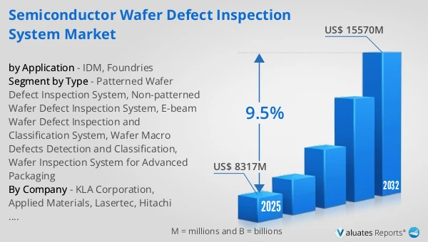
Figure 13. Global Semiconductor Wafer Defect Inspection System Production Value (US$ Million), 2021 vs 2025 vs 2032
Figure 14. Global Semiconductor Wafer Defect Inspection System Production Value (US$ Million), 2021–2032
Figure 15. Global Semiconductor Wafer Defect Inspection System Production Capacity (Units), 2021–2032
Figure 16. Global Semiconductor Wafer Defect Inspection System Production (Units), 2021–2032
Figure 17. Global Semiconductor Wafer Defect Inspection System Average Price (US$/Unit), 2021–2032
Figure 18. Semiconductor Wafer Defect Inspection System Report Years Considered
Figure 19. Semiconductor Wafer Defect Inspection System Production Share by Manufacturers in 2025
Figure 20. Global Semiconductor Wafer Defect Inspection System Production Value Share by Manufacturers (2025)
Figure 21. Semiconductor Wafer Defect Inspection System Market Share by Company Type (Tier 1, Tier 2, and Tier 3): 2021 vs 2025
Figure 22. Top 5 and Top 10 Global Players: Market Share by Semiconductor Wafer Defect Inspection System Revenue in 2025
Figure 23. Global Semiconductor Wafer Defect Inspection System Production Value by Region: 2021 vs 2025 vs 2032 (US$ Million)
Figure 24. Global Semiconductor Wafer Defect Inspection System Production Value Market Share by Region: 2021 vs 2025 vs 2032
Figure 25. Global Semiconductor Wafer Defect Inspection System Production Comparison by Region: 2021 vs 2025 vs 2032 (Units)
Figure 26. Global Semiconductor Wafer Defect Inspection System Production Market Share by Region: 2021 vs 2025 vs 2032
Figure 27. North America Semiconductor Wafer Defect Inspection System Production Value (US$ Million) Growth Rate (2021–2032)
Figure 28. Europe Semiconductor Wafer Defect Inspection System Production Value (US$ Million) Growth Rate (2021–2032)
Figure 29. China Semiconductor Wafer Defect Inspection System Production Value (US$ Million) Growth Rate (2021–2032)
Figure 30. Japan Semiconductor Wafer Defect Inspection System Production Value (US$ Million) Growth Rate (2021–2032)
Figure 31. South Korea Semiconductor Wafer Defect Inspection System Production Value (US$ Million) Growth Rate (2021–2032)
Figure 32. China Taiwan Semiconductor Wafer Defect Inspection System Production Value (US$ Million) Growth Rate (2021–2032)
Figure 33. Southeast Asia Semiconductor Wafer Defect Inspection System Production Value (US$ Million) Growth Rate (2021–2032)
Figure 34. Global Semiconductor Wafer Defect Inspection System Consumption by Region: 2021 vs 2025 vs 2032 (Units)
Figure 35. Global Semiconductor Wafer Defect Inspection System Consumption Market Share by Region: 2021 vs 2025 vs 2032
Figure 36. North America Semiconductor Wafer Defect Inspection System Consumption and Growth Rate (Units), 2021–2032
Figure 37. North America Semiconductor Wafer Defect Inspection System Consumption Market Share by Country (2021–2032)
Figure 38. U.S. Semiconductor Wafer Defect Inspection System Consumption and Growth Rate (Units), 2021–2032
Figure 39. Canada Semiconductor Wafer Defect Inspection System Consumption and Growth Rate (Units), 2021–2032
Figure 40. Europe Semiconductor Wafer Defect Inspection System Consumption and Growth Rate (Units), 2021–2032
Figure 41. Europe Semiconductor Wafer Defect Inspection System Consumption Market Share by Country (2021–2032)
Figure 42. Germany Semiconductor Wafer Defect Inspection System Consumption and Growth Rate (Units), 2021–2032
Figure 43. France Semiconductor Wafer Defect Inspection System Consumption and Growth Rate (Units), 2021–2032
Figure 44. U.K. Semiconductor Wafer Defect Inspection System Consumption and Growth Rate (Units), 2021–2032
Figure 45. Italy Semiconductor Wafer Defect Inspection System Consumption and Growth Rate (Units), 2021–2032
Figure 46. Russia Semiconductor Wafer Defect Inspection System Consumption and Growth Rate (Units), 2021–2032
Figure 47. Asia Pacific Semiconductor Wafer Defect Inspection System Consumption and Growth Rate (Units), 2021–2032
Figure 48. Asia Pacific Semiconductor Wafer Defect Inspection System Consumption Market Share by Region (2021–2032)
Figure 49. China Semiconductor Wafer Defect Inspection System Consumption and Growth Rate (Units), 2021–2032
Figure 50. Japan Semiconductor Wafer Defect Inspection System Consumptio