FEATURED COMPANIES
DuPont
Honeywell
IBIDEN
Shin-Etsu Chemical
Sumco
GlobalWafers
Siltronic
JSR
Dongjin Semichem
Fujifilm
JX Nippon Mining & Metals
Tosoh
Linde
Taiyo Nippon Sanso
Guangdong Huate Gas
Toppan
Unimicron
Samsung Electro-Mechanics
Kinsus Interconnect
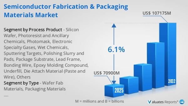
Semiconductor Fabrication & Packaging Materials Market Size
The global Semiconductor Fabrication & Packaging Materials market was valued at US$ 70900 million in 2025 and is anticipated to reach US$ 107175 million by 2032, at a CAGR of 6.1% from 2026 to 2032.
Semiconductor Fabrication & Packaging Materials Market
Semiconductor manufacturing materials and packaging materials are core functional materials that support the entire process of semiconductor device design, wafer fabrication, and chip packaging and testing. Corresponding to the front-end manufacturing processes and back-end packaging processes of the semiconductor industry chain respectively, they jointly determine the performance, yield and reliability of chips.
Semiconductor manufacturing materials refer to various materials used in the wafer fabrication (front-end process) stage to complete core procedures such as photolithography, etching, thin film deposition, doping, cleaning and planarization of wafers. They serve as the foundation for forming the core circuits and functional structures of chips. Such materials must meet stringent requirements including ultra-high purity, precise electrical, optical and chemical properties, and high compatibility with silicon wafers/substrates. They directly affect the integration level, power consumption and stability of chips. Key categories of manufacturing materials include: silicon wafers, photoresists and auxiliary materials, photomasks, specialty electronic gases, wet electronic chemicals, sputtering targets, and polishing slurries and pads.
Semiconductor packaging materials refer to materials used in the chip packaging and testing (back-end process) stage to realize chip fixation, protection, interconnection, heat dissipation and signal transmission. Their function is to convert bare chips cut from wafers into practical integrated circuit (IC) products, enhancing the environmental adaptability and usability of chips. Such materials must balance mechanical strength, thermal conductivity, electrical insulation and temperature-humidity resistance, and be compatible with different packaging formats (e.g., DIP, SOP, QFP, BGA, SiP, Fan-out, etc.). Key categories of packaging materials include: packaging substrates, lead frames, bonding wires, epoxy molding compounds (EMC), underfill and die attach materials.
Market Overview
The global semiconductor materials market maintains a steady growth trajectory. Among them, semiconductor manufacturing materials dominate with a share of approximately 63%, while packaging materials, as an emerging force, account for 37%. Regionally, the Asia-Pacific region leads the world due to its high concentration of manufacturing and packaging capacity, with Taiwan China, Mainland China, Japan, and South Korea forming core industrial clusters. In terms of consumption value by region, Taiwan China, Mainland China, and South Korea remain the top three.
Product Structure Overview
1) Manufacturing Materials
Silicon wafers hold the largest share and serve as the fundamental carrier for semiconductor devices. As a core material for advanced processes, 12-inch large-size silicon wafers maintain stable demand. Following closely are specialty electronic gases and photomasks. The former is widely used in core processes such as photolithography and etching, with ultra-high purity being critical to yield; the latter acts as a template for photolithography processes, and EUV-compatible photomasks feature extremely high technical barriers and significant market concentration.
2) Packaging Materials
Packaging substrates occupy a core position and are irreplaceable in high-density interconnection and System-in-Package (SiP) applications, with their share expected to increase steadily year by year. Key product categories include lead frames, bonding wires, epoxy molding compounds (EMC), underfill adhesives, and die attach materials, each adapted to different packaging scenarios. The bonding wire market presents diversified competition: gold wires dominate the high-end segment, while copper wires and palladium-plated copper wires are gradually replacing gold wires in the mid-to-low-end market. As the mainstream packaging resin, EMC boasts mature processes and significant cost advantages.
Development Trends and Challenges
1) Technological Advancement: Advanced manufacturing processes drive growing demand for high-end materials such as EUV photoresists, large-size silicon wafers, and high-density packaging substrates, with material performance upgrading toward low dielectric constant, high thermal conductivity, and high temperature resistance.
2) Product Diversification: The application of third-generation semiconductor materials is accelerating, with compound materials like silicon carbide (SiC) and gallium nitride (GaN) gaining higher penetration in specific fields. The material system is shifting from silicon-based dominance to diversified development.
3) Regional Synergy: The global industrial focus continues to shift to the Asia-Pacific region, with China emerging as a core area for capacity investment and material consumption, and localized supply chains gradually improving.
Meanwhile, the industry faces multiple challenges: geopolitical conflicts disrupt the stability of global supply chains, and trade frictions restrict imports of certain materials; core technologies for high-end materials are still monopolized by a handful of international enterprises, with intensive patent layouts forming high competitive barriers; fluctuations in raw material prices and stricter environmental regulations increase enterprises' production costs and compliance pressures; the rapid pace of technological iteration requires enterprises to continuously increase R&D investment to meet product update demands.
This report delivers a comprehensive overview of the global Semiconductor Fabrication & Packaging Materials market, with both quantitative and qualitative analyses, to help readers develop growth strategies, assess the competitive landscape, evaluate their position in the current market, and make informed business decisions regarding Semiconductor Fabrication & Packaging Materials. The Semiconductor Fabrication & Packaging Materials market size, estimates, and forecasts are provided in terms of revenue (US$ millions), with 2025 as the base year and historical and forecast data for 2021–2032.
The report segments the global Semiconductor Fabrication & Packaging Materials market comprehensively. Regional market sizes by Type, by Application, by Process Product, and by player are also provided. For deeper insight, the report profiles the competitive landscape, key competitors, and their respective market rankings, and discusses technological trends and new product developments.
This report will assist Semiconductor Fabrication & Packaging Materials manufacturers, new entrants, and companies across the industry value chain with information on revenues, sales volume, and average prices for the overall market and its sub-segments, by company, by Type, by Application, and by region.
Market Segmentation
Scope of Semiconductor Fabrication & Packaging Materials Market Report
| Report Metric |
Details |
| Report Name |
Semiconductor Fabrication & Packaging Materials Market |
| Accounted market size in 2025 |
US$ 70900 in million |
| Forecasted market size in 2032 |
US$ 107175 million |
| CAGR |
6.1% |
| Base Year |
2025 |
| Forecasted years |
2026 - 2032 |
| Segment by Type |
- Wafer Fab Materials
- Packaging Materials
|
| Segment by Process Product |
- Silicon Wafer
- Photoresist and Ancillary Chemicals
- Photomask
- Electronic Specialty Gases
- Wet Chemicals
- Sputtering Targets
- Polishing Slurry and Pads
- Package Substrate
- Lead Frame
- Bonding Wire
- Epoxy Molding Compound
- Underfill
- Die Attach Material (Paste and Wire)
- Others
|
| Segment by Application |
- Memory
- Logic
- Analog
- Discrete Device & Sensor
- Others
|
| By Region |
- North America (United States, Canada)
- Europe (Germany, France, UK, Italy, Russia) Rest of Europe
- Nordic Countries
- Asia-Pacific (China, Japan, South Korea)
- Southeast Asia (India, Australia)
- Rest of Asia
- Latin America (Mexico, Brazil)
- Rest of Latin America
- Middle East & Africa (Turkey, Saudi Arabia, UAE, Rest of MEA)
|
| By Company |
3M, Advanced Assembly Materials International, AGC, AIM Solder, Allresist GmbH, AMETEK (Coining), Anjimirco Shanghai, APS Holdings, AT&S, Athene, Chang Wah Technology, ChemChina, CMC Materials, Inc., Daeduck Electronics, Dai Nippon Printing (DNP), Darwin, Dongjin Semichem, DuPont, Enomoto, Eternal Materials, FNS TECH Co., LTD, FOJIBO, FST Corporation, Fuji Chemical, Fujifilm, Fujimi Incorporated, Fusheng Electronics, Futurrex, GlobalWafers, Grinm Advanced Materials Co., Ltd., Guangdong Huate Gas, HAESUNG DS, Henkel, Heraeu, Honeywell, Hubei Dinglong Co.,Ltd, Hyosung, Ibiden, JSR, JX Advanced Metals, Kangqiang Electronics, Kanto Denka Kogyo, KC Tech, KCC, Kinsus Interconnect, Konfoong Materials International, Kyocera, LG InnoTek, Linde, LORD Corporation, MacDermid Alpha, Materion, Merck (Versum Materials), Mitsui Chemical, MK Electron, NAGASE, NAMICS, National Silicon Industry Group (NSIG), Nippon Micrometal Corporation, Panasonic, PERIC, Plansee SE, Poongwon, POSSEHL, Power Stencil, Proterial, Resonac, Samsung Electro-Mechanics, Sewoo incorporation, Shandong FeiYuan, Shenmao Technology, Shennan Circuit, Shenzhen Fastprint Circuit Tech, Shin-Etsu Chemical, Shinko Electric Industries, Siltronic AG, SK Materials (SK specialty), SK Siltron, SKC, SMIC Senju Metal Industry Co., Ltd, Soitec, Soulbrain, SUMCO, Sumitomo Bakelite, Sumitomo Chemical, Sunstar, Taiyo Nippon Sanso, Tamura, TANAKA Precious Metals, TATSUTA Group, TOKYO OHKA KOGYO (TOK), TOPPAN, TOSOH, TWI Incorporated, ULVAC, Unimicron, Wafer Works Corporation, Wave Electronics, Won Chemical, Zhen Ding Technology, Zhonghuan Advanced Semiconductor Materials, Zhuhai Access Semiconductor |
| Forecast units |
USD million in value |
| Report coverage |
Revenue and volume forecast, company share, competitive landscape, growth factors and trends |
Chapter Outline
- Chapter 1: Defines the scope of the report and presents an executive summary of market segments (by Type, by Application, by Process Product, etc.), including the size of each segment and its future growth potential. It offers a high-level view of the current market and its likely evolution in the short, medium, and long term.
- Chapter 2: Summarizes global and regional market size and outlines market dynamics and recent developments, including key drivers, restraints, challenges and risks for industry participants, and relevant policy analysis.
- Chapter 3: Provides a detailed view of the competitive landscape for Semiconductor Fabrication & Packaging Materials companies, covering revenue share, development plans, and mergers and acquisitions.
- Chapter 4: Analyzes segments by Type, detailing the size and growth potential of each segment to help readers identify blue-ocean opportunities.
- Chapter 5: Analyzes segments by Application, detailing the size and growth potential of each downstream segment to help readers identify blue-ocean opportunities.
- Chapter 6–10: Regional deep dives (North America, Europe, Asia Pacific, Latin America, Middle East & Africa) broken down by country. Each chapter quantifies market size and growth potential by region and key countries, and outlines market development, outlook, addressable space, and capacity.
- Chapter 11: Profiles key players, presenting essential information on leading companies, including product/ service offerings, revenue, gross margin, product introductions/portfolios, recent developments, etc.
- Chapter 12: Key findings and conclusions of the report.
FAQ for this report
How fast is Semiconductor Fabrication & Packaging Materials Market growing?
Ans: The Semiconductor Fabrication & Packaging Materials Market witnessing a CAGR of 6.1% during the forecast period 2026-2032.
What is the Semiconductor Fabrication & Packaging Materials Market size in 2032?
Ans: The Semiconductor Fabrication & Packaging Materials Market size in 2032 will be US$ 107175 million.
Who are the main players in the Semiconductor Fabrication & Packaging Materials Market report?
Ans: The main players in the Semiconductor Fabrication & Packaging Materials Market are 3M, Advanced Assembly Materials International, AGC, AIM Solder, Allresist GmbH, AMETEK (Coining), Anjimirco Shanghai, APS Holdings, AT&S, Athene, Chang Wah Technology, ChemChina, CMC Materials, Inc., Daeduck Electronics, Dai Nippon Printing (DNP), Darwin, Dongjin Semichem, DuPont, Enomoto, Eternal Materials, FNS TECH Co., LTD, FOJIBO, FST Corporation, Fuji Chemical, Fujifilm, Fujimi Incorporated, Fusheng Electronics, Futurrex, GlobalWafers, Grinm Advanced Materials Co., Ltd., Guangdong Huate Gas, HAESUNG DS, Henkel, Heraeu, Honeywell, Hubei Dinglong Co.,Ltd, Hyosung, Ibiden, JSR, JX Advanced Metals, Kangqiang Electronics, Kanto Denka Kogyo, KC Tech, KCC, Kinsus Interconnect, Konfoong Materials International, Kyocera, LG InnoTek, Linde, LORD Corporation, MacDermid Alpha, Materion, Merck (Versum Materials), Mitsui Chemical, MK Electron, NAGASE, NAMICS, National Silicon Industry Group (NSIG), Nippon Micrometal Corporation, Panasonic, PERIC, Plansee SE, Poongwon, POSSEHL, Power Stencil, Proterial, Resonac, Samsung Electro-Mechanics, Sewoo incorporation, Shandong FeiYuan, Shenmao Technology, Shennan Circuit, Shenzhen Fastprint Circuit Tech, Shin-Etsu Chemical, Shinko Electric Industries, Siltronic AG, SK Materials (SK specialty), SK Siltron, SKC, SMIC Senju Metal Industry Co., Ltd, Soitec, Soulbrain, SUMCO, Sumitomo Bakelite, Sumitomo Chemical, Sunstar, Taiyo Nippon Sanso, Tamura, TANAKA Precious Metals, TATSUTA Group, TOKYO OHKA KOGYO (TOK), TOPPAN, TOSOH, TWI Incorporated, ULVAC, Unimicron, Wafer Works Corporation, Wave Electronics, Won Chemical, Zhen Ding Technology, Zhonghuan Advanced Semiconductor Materials, Zhuhai Access Semiconductor
What are the Application segmentation covered in the Semiconductor Fabrication & Packaging Materials Market report?
Ans: The Applications covered in the Semiconductor Fabrication & Packaging Materials Market report are Memory, Logic, Analog, Discrete Device & Sensor, Others
What are the Type segmentation covered in the Semiconductor Fabrication & Packaging Materials Market report?
Ans: The Types covered in the Semiconductor Fabrication & Packaging Materials Market report are Wafer Fab Materials, Packaging Materials