FEATURED COMPANIES
LB Semicon Inc
FINECS
Amkor Technology
ASE
Raytek Semiconductor,Inc.
Winstek Semiconductor
Nepes
sj company co., LTD.
SJ Semiconductor Co
Chipbond
Chip More
ChipMOS
Shenzhen Tongxingda Technology
MacDermid Alpha Electronics
Jiangsu CAS Microelectronics Integration
Tianshui Huatian Technology
JCET Group
Unisem Group
Powertech Technology Inc
SFA Semicon
International Micro Industries
Jiangsu nepes Semiconductor
Jiangsu Yidu Technology
Intel
SAMSUNG
TSMC
CuNiAu Bumping Market Size
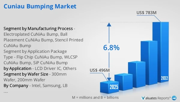
The global CuNiAu Bumping market was valued at US$ 496 million in 2025 and is anticipated to reach US$ 783 million by 2032, at a CAGR of 6.8% from 2026 to 2032.
CuNiAu Bumping Market
The 2025 U.S. tariff policies introduce profound uncertainty into the global economic landscape. This report critically examines the implications of recent tariff adjustments and international strategic countermeasures on CuNiAu Bumping competitive dynamics, regional economic interdependencies, and supply chain reconfigurations.
CuNiAu bumping refers to a high-reliability, multi-layer metallization process used in advanced semiconductor packaging, where a copper (Cu) pillar is formed on the wafer surface, followed by a nickel (Ni) barrier layer and a gold (Au) capping layer. This bumping structure offers excellent electrical conductivity, oxidation resistance, and thermal stability, making it ideal for fine-pitch interconnects and advanced integration schemes. CuNiAu bumps are typically fabricated via electroplating and can be classified into standard-size bumps (>100 μm), micro-bumps (40–100 μm), and ultra-fine-pitch bumps (<40 μm), depending on the application. They are widely used in Flip Chip packaging, wafer-level packaging (WLP), through-silicon via (TSV) interconnects, die-to-die (D2D), die-to-wafer (D2W), and chiplet integration platforms where strong interfacial bonding and high I/O density are critical.
As semiconductor packaging trends shift toward heterogeneous integration, 3D stacking, and chiplet architectures, CuNiAu bumping is gaining strategic importance due to its compatibility with thermo-compression bonding (TCB), Au–Au diffusion bonding, and hybrid bonding technologies. The Ni layer acts as an effective diffusion barrier to prevent copper migration and solder interaction, while the Au cap ensures robust, low-resistance bonding, even under high-temperature or low-pressure processes. With the rise of AI accelerators, high-bandwidth memory (HBM), photonic-electronic co-packaging (CPO) and next-generation logic devices, the demand for ultra-fine, high-reliability micro-bumps is accelerating.
This report delivers a comprehensive overview of the global CuNiAu Bumping market, with both quantitative and qualitative analyses, to help readers develop growth strategies, assess the competitive landscape, evaluate their position in the current market, and make informed business decisions regarding CuNiAu Bumping. The CuNiAu Bumping market size, estimates, and forecasts are provided in terms of output/shipments (K Wafers) and revenue (US$ millions), with 2025 as the base year and historical and forecast data for 2021–2032.
The report segments the global CuNiAu Bumping market comprehensively. Regional market sizes by Wafer Size, by Application, by Manufacturing Process, and by company are also provided. For deeper insight, the report profiles the competitive landscape, key competitors, and their respective market rankings, and discusses technological trends and new product developments.
This report will assist CuNiAu Bumping manufacturers, new entrants, and companies across the industry value chain with information on revenues, production, and average prices for the overall market and its sub-segments, by company, by Wafer Size, by Application, and by region.
Market Segmentation
Scope of CuNiAu Bumping Market Report
| Report Metric |
Details |
| Report Name |
CuNiAu Bumping Market |
| Accounted market size in 2025 |
US$ 496 million |
| Forecasted market size in 2032 |
US$ 783 million |
| CAGR |
6.8% |
| Base Year |
2025 |
| Forecasted years |
2026 - 2032 |
| Segment by Wafer Size |
|
| Segment by Manufacturing Process |
- Electroplated CuNiAu Bump
- Ball Placement CuNiAu Bump
- Stencil Printed CuNiAu Bump
|
| Segment by Application Package Type |
- Flip Chip CuNiAu Bump
- WLCSP CuNiAu Bump
- SiP CuNiAu Bump
|
| by Application |
|
| Production by Region |
- South Korea
- Europe
- China
- Japan
- China Taiwan
|
| Consumption by Region |
- North America (United States, Canada)
- Europe (Germany, France, UK, Italy, Russia)
- Asia-Pacific (China, Japan, South Korea, Taiwan)
- Southeast Asia (India)
- Latin America (Mexico, Brazil)
|
| By Company |
Intel, Samsung, LB Semicon Inc, TSMC, FINECS, Amkor Technology, ASE, Raytek Semiconductor,Inc., Winstek Semiconductor, Nepes, JCET Group, sj company co., LTD., SJ Semiconductor Co, Chipbond, Chip More, ChipMOS, Shenzhen Tongxingda Technology, MacDermid Alpha Electronics, Jiangsu CAS Microelectronics Integration, Tianshui Huatian Technology, Jiangsu Yidu Technology, Unisem Group, Powertech Technology Inc., SFA Semicon, International Micro Industries, Jiangsu nepes Semiconductor |
| Forecast units |
USD million in value |
| Report coverage |
Revenue and volume forecast, company share, competitive landscape, growth factors and trends |
Chapter Outline
- Chapter 1: Defines the scope of the report and presents an executive summary of market segments (by Wafer Size, by Application, by Manufacturing Process, etc.), including the size of each segment and its future growth potential. It offers a high-level view of the current market and its likely evolution in the short, medium, and long term.
- Chapter 2: Provides a detailed analysis of the competitive landscape for CuNiAu Bumping manufacturers, including prices, production, value-based market shares, latest development plans, and information on mergers and acquisitions.
- Chapter 3: Examines CuNiAu Bumping production/output and value by region and country, providing a quantitative assessment of market size and growth potential for each region over the next six years.
- Chapter 4: Analyzes CuNiAu Bumping consumption at the regional and country levels. It quantifies market size and growth potential for each region and its key countries, and outlines market development, outlook, addressable space, and national production.
- Chapter 5: Analyzes market segments by Wafer Size, covering the size and growth potential of each segment to help readers identify “blue ocean” opportunities.
- Chapter 6: Analyzes market segments by Application, covering the size and growth potential of each segment to help readers identify “blue ocean” opportunities in downstream markets.
- Chapter 7: Profiles key players, detailing the fundamentals of major companies, including product production/output, value, price, gross margin, product portfolio/introductions, and recent developments.
- Chapter 8: Reviews the industry value chain, including upstream and downstream segments.
- Chapter 9: Discusses market dynamics and recent developments, including drivers, restraints, challenges and risks for manufacturers, U.S. Tariffs and relevant policy analysis.
- Chapter 10: Summarizes the key findings and conclusions of the report.
FAQ for this report
How fast is CuNiAu Bumping Market growing?
Ans: The CuNiAu Bumping Market witnessing a CAGR of 6.8% during the forecast period 2026-2032.
What is the CuNiAu Bumping Market size in 2032?
Ans: The CuNiAu Bumping Market size in 2032 will be US$ 783 million.
Who are the main players in the CuNiAu Bumping Market report?
Ans: The main players in the CuNiAu Bumping Market are Intel, Samsung, LB Semicon Inc, TSMC, FINECS, Amkor Technology, ASE, Raytek Semiconductor,Inc., Winstek Semiconductor, Nepes, JCET Group, sj company co., LTD., SJ Semiconductor Co, Chipbond, Chip More, ChipMOS, Shenzhen Tongxingda Technology, MacDermid Alpha Electronics, Jiangsu CAS Microelectronics Integration, Tianshui Huatian Technology, Jiangsu Yidu Technology, Unisem Group, Powertech Technology Inc., SFA Semicon, International Micro Industries, Jiangsu nepes Semiconductor
What are the Application segmentation covered in the CuNiAu Bumping Market report?
Ans: The Applications covered in the CuNiAu Bumping Market report are LCD Driver IC, Others
What are the Type segmentation covered in the CuNiAu Bumping Market report?
Ans: The Types covered in the CuNiAu Bumping Market report are Flip Chip CuNiAu Bump, WLCSP CuNiAu Bump, SiP CuNiAu Bump
FEATURED COMPANIES
LB Semicon Inc
FINECS
Amkor Technology
ASE
Raytek Semiconductor,Inc.
Winstek Semiconductor
Nepes
sj company co., LTD.
SJ Semiconductor Co
Chipbond
Chip More
ChipMOS
Shenzhen Tongxingda Technology
MacDermid Alpha Electronics
Jiangsu CAS Microelectronics Integration
Tianshui Huatian Technology
JCET Group
Unisem Group
Powertech Technology Inc
SFA Semicon
International Micro Industries
Jiangsu nepes Semiconductor
Jiangsu Yidu Technology
Intel
SAMSUNG
TSMC