FEATURED COMPANIES
LB Semicon Inc
FINECS
Amkor Technology
ASE
Raytek Semiconductor,Inc.
Winstek Semiconductor
Nepes
JiangYin ChangDian Advanced Packaging
sj company co., LTD.
SJ Semiconductor Co
Chipbond
Chip More
ChipMOS
Shenzhen Tongxingda Technology
Jiangsu CAS Microelectronics Integration
Tianshui Huatian Technology
Unisem Group
Powertech Technology Inc
SFA Semicon
International Micro Industries
Jiangsu nepes Semiconductor
Jiangsu Yidu Technology
Intel
SAMSUNG
TSMC
Sn Bumping Market Size
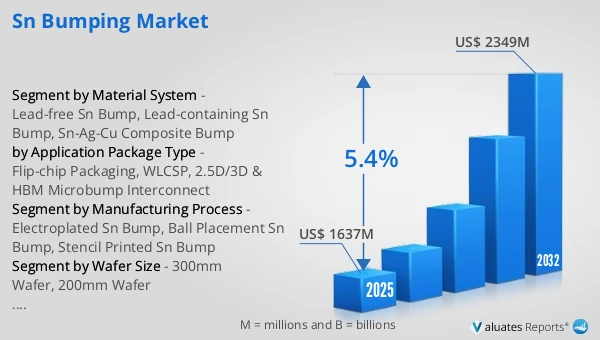
The global Sn Bumping market was valued at US$ 1637 million in 2025 and is anticipated to reach US$ 2349 million by 2032, at a CAGR of 5.4% from 2026 to 2032.
Sn Bumping Market
The 2025 U.S. tariff policies introduce profound uncertainty into the global economic landscape. This report critically examines the implications of recent tariff adjustments and international strategic countermeasures on Sn Bumping competitive dynamics, regional economic interdependencies, and supply chain reconfigurations.
Sn Bumping (Tin Bumping) is a widely used interconnect technology in semiconductor packaging, where tin-based solder bumps are formed on wafer pads to enable flip-chip bonding and wafer-level packaging. These bumps serve as electrical and mechanical connections between the chip and the substrate or interposer. Sn bumps are typically fabricated through electroplating, stencil printing, or ball placement with subsequent reflow, and are often composed of pure tin (Sn), eutectic SnPb, or lead-free alloys such as SnAg or SnAgCu (SAC). Sn Bumping can be classified into standard solder balls (for flip-chip and BGA), micro solder bumps (for fine-pitch and WLCSP), and Sn caps atop copper pillars or other bump structures, enabling compatibility with a wide range of packaging architectures.
Technically, mass-production Sn bumping is an integrated stack of UBM (under-bump metallurgy) + bump formation + reflow/reshaping + metrology/inspection. Public OSAT documentation describes solder bumps being formed via thin-film metal deposition, electroplating, and ball loading/ball placement techniques; stencil/paste printing is also an established route and is often discussed as a cost-advantaged option, but ultra-fine pitch pushes tighter process windows and defect controls. In WLCSP implementations, an UBM is added and solder bumps are placed directly over die I/O pads, enabling standard surface-mount reflow assembly downstream.
In applications and market dynamics, Sn bumps remain foundational for flip-chip packaging and WLCSP, and extend into high-density microbump interconnect for 3D/stacked products (e.g., HBM and other advanced 3D packaging). The competitive base is concentrated in leading OSATs and advanced-packaging ecosystems; ASE and Amkor both publicly position wafer bumping as essential for flip-chip/WLCSP and offer 200mm/300mm bumping with multiple process routes. Key trends/drivers include: (1) finer pitch and higher I/O density accelerating adoption of Cu pillar + solder/Sn cap for tighter control of joint diameter and stand-off; (2) lead-free solder mainstreaming (Sn-Ag, Sn-Cu, SAC); and (3) rising reliability constraints in advanced packages, including electromigration and IMC-driven failure modes at Cu/Ni-Sn interfaces, requiring co-optimization across materials, UBM, and thermo-mechanical design.
This report delivers a comprehensive overview of the global Sn Bumping market, with both quantitative and qualitative analyses, to help readers develop growth strategies, assess the competitive landscape, evaluate their position in the current market, and make informed business decisions regarding Sn Bumping. The Sn Bumping market size, estimates, and forecasts are provided in terms of output/shipments (Million Units) and revenue (US$ millions), with 2025 as the base year and historical and forecast data for 2021–2032.
The report segments the global Sn Bumping market comprehensively. Regional market sizes by Wafer Size, by Application Package Type, by Manufacturing Process, and by company are also provided. For deeper insight, the report profiles the competitive landscape, key competitors, and their respective market rankings, and discusses technological trends and new product developments.
This report will assist Sn Bumping manufacturers, new entrants, and companies across the industry value chain with information on revenues, production, and average prices for the overall market and its sub-segments, by company, by Wafer Size, by Application Package Type, and by region.
Market Segmentation
Scope of Sn Bumping Market Report
| Report Metric |
Details |
| Report Name |
Sn Bumping Market |
| Accounted market size in 2025 |
US$ 1637 million |
| Forecasted market size in 2032 |
US$ 2349 million |
| CAGR |
5.4% |
| Base Year |
2025 |
| Forecasted years |
2026 - 2032 |
| Segment by Wafer Size |
|
| Segment by Manufacturing Process |
- Electroplated Sn Bump
- Ball Placement Sn Bump
- Stencil Printed Sn Bump
|
| Segment by Material System |
- Lead-free Sn Bump
- Lead-containing Sn Bump
- Sn-Ag-Cu Composite Bump
|
| by Application Package Type |
- Flip-chip Packaging
- WLCSP
- 2.5D/3D & HBM Microbump Interconnect
|
| Production by Region |
- North America
- Europe
- China
- Japan
- China Taiwan
- South Korea
|
| Consumption by Region |
- North America (United States, Canada)
- Europe (Germany, France, UK, Italy, Russia)
- Asia-Pacific (China, Japan, South Korea, Taiwan)
- Southeast Asia (India)
- Latin America (Mexico, Brazil)
|
| By Company |
ASE, Samsung, LB Semicon Inc, Powertech Technology Inc., TSMC, Amkor Technology, Intel, Raytek Semiconductor,Inc., Winstek Semiconductor, Nepes, JiangYin ChangDian Advanced Packaging, sj company co., LTD., SJ Semiconductor Co, Chipbond, Chip More, ChipMOS, Shenzhen Tongxingda Technology, FINECS, Jiangsu CAS Microelectronics Integration, Tianshui Huatian Technology, Jiangsu nepes Semiconductor, Unisem Group, Jiangsu Yidu Technology, SFA Semicon, International Micro Industries |
| Forecast units |
USD million in value |
| Report coverage |
Revenue and volume forecast, company share, competitive landscape, growth factors and trends |
Chapter Outline
- Chapter 1: Defines the scope of the report and presents an executive summary of market segments (by Wafer Size, by Application Package Type, by Manufacturing Process, etc.), including the size of each segment and its future growth potential. It offers a high-level view of the current market and its likely evolution in the short, medium, and long term.
- Chapter 2: Provides a detailed analysis of the competitive landscape for Sn Bumping manufacturers, including prices, production, value-based market shares, latest development plans, and information on mergers and acquisitions.
- Chapter 3: Examines Sn Bumping production/output and value by region and country, providing a quantitative assessment of market size and growth potential for each region over the next six years.
- Chapter 4: Analyzes Sn Bumping consumption at the regional and country levels. It quantifies market size and growth potential for each region and its key countries, and outlines market development, outlook, addressable space, and national production.
- Chapter 5: Analyzes market segments by Wafer Size, covering the size and growth potential of each segment to help readers identify “blue ocean” opportunities.
- Chapter 6: Analyzes market segments by Application Package Type, covering the size and growth potential of each segment to help readers identify “blue ocean” opportunities in downstream markets.
- Chapter 7: Profiles key players, detailing the fundamentals of major companies, including product production/output, value, price, gross margin, product portfolio/introductions, and recent developments.
- Chapter 8: Reviews the industry value chain, including upstream and downstream segments.
- Chapter 9: Discusses market dynamics and recent developments, including drivers, restraints, challenges and risks for manufacturers, U.S. Tariffs and relevant policy analysis.
- Chapter 10: Summarizes the key findings and conclusions of the report.
FAQ for this report
How fast is Sn Bumping Market growing?
Ans: The Sn Bumping Market witnessing a CAGR of 5.4% during the forecast period 2026-2032.
What is the Sn Bumping Market size in 2032?
Ans: The Sn Bumping Market size in 2032 will be US$ 2349 million.
Who are the main players in the Sn Bumping Market report?
Ans: The main players in the Sn Bumping Market are ASE, Samsung, LB Semicon Inc, Powertech Technology Inc., TSMC, Amkor Technology, Intel, Raytek Semiconductor,Inc., Winstek Semiconductor, Nepes, JiangYin ChangDian Advanced Packaging, sj company co., LTD., SJ Semiconductor Co, Chipbond, Chip More, ChipMOS, Shenzhen Tongxingda Technology, FINECS, Jiangsu CAS Microelectronics Integration, Tianshui Huatian Technology, Jiangsu nepes Semiconductor, Unisem Group, Jiangsu Yidu Technology, SFA Semicon, International Micro Industries
What are the Application segmentation covered in the Sn Bumping Market report?
Ans: The Applications covered in the Sn Bumping Market report are Flip-chip Packaging, WLCSP, 2.5D/3D & HBM Microbump Interconnect
What are the Type segmentation covered in the Sn Bumping Market report?
Ans: The Types covered in the Sn Bumping Market report are Flip-chip Packaging, WLCSP, 2.5D/3D & HBM Microbump Interconnect
FEATURED COMPANIES
LB Semicon Inc
FINECS
Amkor Technology
ASE
Raytek Semiconductor,Inc.
Winstek Semiconductor
Nepes
JiangYin ChangDian Advanced Packaging
sj company co., LTD.
SJ Semiconductor Co
Chipbond
Chip More
ChipMOS
Shenzhen Tongxingda Technology
Jiangsu CAS Microelectronics Integration
Tianshui Huatian Technology
Unisem Group
Powertech Technology Inc
SFA Semicon
International Micro Industries
Jiangsu nepes Semiconductor
Jiangsu Yidu Technology
Intel
SAMSUNG
TSMC