FEATURED COMPANIES
LB Semicon Inc
Nepes
Gold Bump Market Size
The global Gold Bump market was valued at US$ 558 million in 2025 and is anticipated to reach US$ 873 million by 2032, at a CAGR of 5.7% from 2026 to 2032.
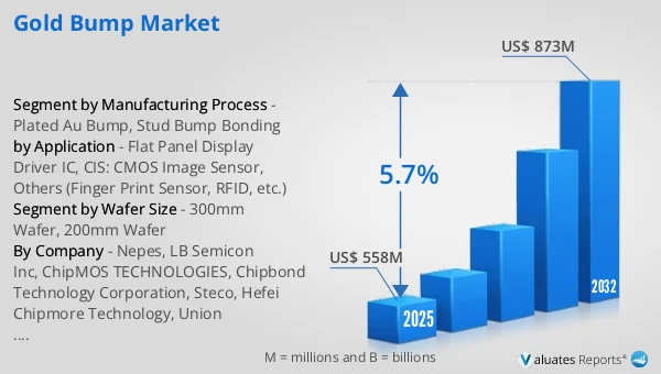
Gold Bump Market
The 2025 U.S. tariff policies introduce profound uncertainty into the global economic landscape. This report critically examines the implications of recent tariff adjustments and international strategic countermeasures on Gold Bump competitive dynamics, regional economic interdependencies, and supply chain reconfigurations.
Gold Bump technology refers to the formation of tiny gold protrusions on semiconductor dies, typically used as interconnect structures in high-density packaging and display driver IC (DDI) applications. These bumps are fabricated via electroplating or stud bump bonding (SBB), offering superior electrical conductivity, excellent resistance to oxidation, and high mechanical reliability. Gold bumps are essential in ultra-fine pitch interconnections where traditional solder bumps are no longer feasible. They are broadly classified into plated gold bumps—used in high-throughput wafer-level processes—and stud gold bumps, which are more suitable for small-batch, high-mix environments. Gold bumping is extensively deployed in COF (Chip-on-Film), COG (Chip-on-Glass), CSP (Chip Scale Package), CMOS image sensors, MEMS, optical modules, and fingerprint sensors, especially where bump uniformity, planarity, and fine-pitch control are critical.
With the rising demand for high-resolution displays, wearable electronics, 3D sensing modules, and ultra-compact mobile devices, Gold Bump technology is evolving toward sub-20 μm pitch, thinner bump height, improved bump coplanarity, and integration with hybrid bonding and thermo-compression bonding (TCB) for advanced heterogeneous packaging. Innovations such as AuSn alloy bumping are also being explored to enhance joint reliability and reflow compatibility.
This report delivers a comprehensive overview of the global Gold Bump market, with both quantitative and qualitative analyses, to help readers develop growth strategies, assess the competitive landscape, evaluate their position in the current market, and make informed business decisions regarding Gold Bump. The Gold Bump market size, estimates, and forecasts are provided in terms of output/shipments (K Wafers) and revenue (US$ millions), with 2025 as the base year and historical and forecast data for 2021–2032.
The report segments the global Gold Bump market comprehensively. Regional market sizes by Wafer Size, by Application, by Manufacturing Process, and by company are also provided. For deeper insight, the report profiles the competitive landscape, key competitors, and their respective market rankings, and discusses technological trends and new product developments.
This report will assist Gold Bump manufacturers, new entrants, and companies across the industry value chain with information on revenues, production, and average prices for the overall market and its sub-segments, by company, by Wafer Size, by Application, and by region.
Market Segmentation
Scope of Gold Bump Market Report
| Report Metric |
Details |
| Report Name |
Gold Bump Market |
| Accounted market size in 2025 |
US$ 558 million |
| Forecasted market size in 2032 |
US$ 873 million |
| CAGR |
5.7% |
| Base Year |
2025 |
| Forecasted years |
2026 - 2032 |
| Segment by Wafer Size |
|
| Segment by Manufacturing Process |
- Plated Au Bump
- Stud Bump Bonding
|
| by Application |
- Flat Panel Display Driver IC
- CIS: CMOS Image Sensor
- Others (Finger Print Sensor, RFID, etc.)
|
| Production by Region |
- South Korea
- China
- China Taiwan
|
| Consumption by Region |
- North America (United States, Canada)
- Europe (Germany, France, UK, Italy, Russia)
- Asia-Pacific (China, Japan, South Korea, Taiwan)
- Southeast Asia (India)
- Latin America (Mexico, Brazil)
|
| By Company |
Nepes, LB Semicon Inc, ChipMOS TECHNOLOGIES, Chipbond Technology Corporation, Steco, Hefei Chipmore Technology, Union Semiconductor (Hefei) Co., Ltd., Shenzhen TXD Technology, Jiangsu Yidu Technology, Tongfu Microelectronics (TFME), China Wafer Level CSP Co., Ltd |
| Forecast units |
USD million in value |
| Report coverage |
Revenue and volume forecast, company share, competitive landscape, growth factors and trends |
Chapter Outline
- Chapter 1: Defines the scope of the report and presents an executive summary of market segments (by Wafer Size, by Application, by Manufacturing Process, etc.), including the size of each segment and its future growth potential. It offers a high-level view of the current market and its likely evolution in the short, medium, and long term.
- Chapter 2: Provides a detailed analysis of the competitive landscape for Gold Bump manufacturers, including prices, production, value-based market shares, latest development plans, and information on mergers and acquisitions.
- Chapter 3: Examines Gold Bump production/output and value by region and country, providing a quantitative assessment of market size and growth potential for each region over the next six years.
- Chapter 4: Analyzes Gold Bump consumption at the regional and country levels. It quantifies market size and growth potential for each region and its key countries, and outlines market development, outlook, addressable space, and national production.
- Chapter 5: Analyzes market segments by Wafer Size, covering the size and growth potential of each segment to help readers identify “blue ocean” opportunities.
- Chapter 6: Analyzes market segments by Application, covering the size and growth potential of each segment to help readers identify “blue ocean” opportunities in downstream markets.
- Chapter 7: Profiles key players, detailing the fundamentals of major companies, including product production/output, value, price, gross margin, product portfolio/introductions, and recent developments.
- Chapter 8: Reviews the industry value chain, including upstream and downstream segments.
- Chapter 9: Discusses market dynamics and recent developments, including drivers, restraints, challenges and risks for manufacturers, U.S. Tariffs and relevant policy analysis.
- Chapter 10: Summarizes the key findings and conclusions of the report.
FAQ for this report
How fast is Gold Bump Market growing?
Ans: The Gold Bump Market witnessing a CAGR of 5.7% during the forecast period 2026-2032.
What is the Gold Bump Market size in 2032?
Ans: The Gold Bump Market size in 2032 will be US$ 873 million.
Who are the main players in the Gold Bump Market report?
Ans: The main players in the Gold Bump Market are Nepes, LB Semicon Inc, ChipMOS TECHNOLOGIES, Chipbond Technology Corporation, Steco, Hefei Chipmore Technology, Union Semiconductor (Hefei) Co., Ltd., Shenzhen TXD Technology, Jiangsu Yidu Technology, Tongfu Microelectronics (TFME), China Wafer Level CSP Co., Ltd
What are the Application segmentation covered in the Gold Bump Market report?
Ans: The Applications covered in the Gold Bump Market report are Flat Panel Display Driver IC, CIS: CMOS Image Sensor, Others (Finger Print Sensor, RFID, etc.)