FEATURED COMPANIES
LB Semicon Inc
FINECS
Amkor Technology
ASE
Raytek Semiconductor,Inc.
Nepes
sj company co., LTD.
SJ Semiconductor Co
Chipbond
Chip More
ChipMOS
Shenzhen Tongxingda Technology
Jiangsu CAS Microelectronics Integration
Tianshui Huatian Technology
JCET Group
Unisem Group
Powertech Technology Inc
SFA Semicon
International Micro Industries
Jiangsu nepes Semiconductor
Jiangsu Yidu Technology
Intel
SAMSUNG
Winstek Semiconductor
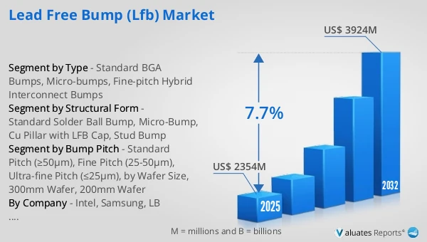
Lead Free Bump (LFB) Market Size
The global Lead Free Bump (LFB) market was valued at US$ 2354 million in 2025 and is anticipated to reach US$ 3924 million by 2032, at a CAGR of 7.7% from 2026 to 2032.
Lead Free Bump (LFB) Market
The 2025 U.S. tariff policies introduce profound uncertainty into the global economic landscape. This report critically examines the implications of recent tariff adjustments and international strategic countermeasures on Lead Free Bump (LFB) competitive dynamics, regional economic interdependencies, and supply chain reconfigurations.
Lead-Free Bump (LFB) generally refers to wafer-level bump interconnects formed with Pb-free solders or Pb-free bump structures to electrically/thermally connect a semiconductor die to a carrier (substrate/interposer) in flip-chip and related advanced packages. EU technical documentation on RoHS exemptions describes flip-chip solder bumps as minute solder spheres connecting the die and carrier, with stress concentrated at the bump interface and transferred to fragile low-k layers. In practice, LFB offerings are commonly grouped into plated solder bumps (C4/SAC-type), Cu-pillar bumps with Pb-free solder caps, and micro-bumps used for high-density 2.5D/3D and chiplet interconnects, often combined with wafer-level repassivation and RDL to support FC-BGA, FC-CSP, WLCSP and advanced packaging stacks.
LFB technology is driven by (1) Pb-free alloy systems, (2) wafer bumping process integration, and (3) reliability engineering. SAC alloys are the mainstream Pb-free choice; Indium explicitly defines SAC305 (96.5Sn/3.0Ag/0.5Cu) as a widely used Pb-free solder developed to comply with regulations such as RoHS. Other Pb-free families (Sn-Cu, Sn-Ag, Sn-Bi, Sn-In, and modified SAC variants) are deployed for cost, low-temperature assembly, or crack-resistance trade-offs. The typical process chain includes UBM deposition/electroplating, lithographic openings, Cu pillar and/or solder plating, reflow shaping, cleaning/inspection, and integration with repassivation and multi-layer RDL. Amkor states its 200/300mm “lead-free and Cu pillar solder compositions” are production-certified, illustrating industrial maturity. Reliability remains the hardest constraint: EU RoHS exemption dossiers emphasize that Pb-containing solders are softer/more ductile and can better absorb CTE-mismatch stress, reducing low-k cracking and solder cracking risks—explaining why legacy high-Pb bumps can persist in certain high-reliability envelopes.
The competitive landscape spans OSATs and packaging leaders, advanced packaging foundries/IDMs, and the materials/chemicals supply chain. On the OSAT side, Amkor and ASE highlight high-volume Pb-free and Cu-pillar bumping capabilities, while the broader market is pulled by chiplet and 2.5D/3D roadmaps. From a technology-trend perspective, MA-tek notes two main paths toward <40µm pitch high-density interconnects—shrinking solder bumps (micro-bumps) versus Cu-Cu bonding—and argues micro-bump approaches remain more practical for many OSATs due to cost/infrastructure barriers, listing Amkor, ASE, Intel, JCET, Samsung, and TSMC as active investors. Market adoption is therefore expanding with advanced packaging volumes, while exemptions and reliability constraints still limit full displacement of Pb-containing bumps in specific “large die / legacy low-k / mission-critical” cases. Key drivers include RoHS-linked compliance pressure, rising I/O density and power requirements in HPC/AI, and sustained capex in wafer-level packaging and bumping capacity.
This report delivers a comprehensive overview of the global Lead Free Bump (LFB) market, with both quantitative and qualitative analyses, to help readers develop growth strategies, assess the competitive landscape, evaluate their position in the current market, and make informed business decisions regarding Lead Free Bump (LFB). The Lead Free Bump (LFB) market size, estimates, and forecasts are provided in terms of output/shipments (K Wafers) and revenue (US$ millions), with 2025 as the base year and historical and forecast data for 2021–2032.
The report segments the global Lead Free Bump (LFB) market comprehensively. Regional market sizes by Type, by Wafer Size, by Structural Form, and by company are also provided. For deeper insight, the report profiles the competitive landscape, key competitors, and their respective market rankings, and discusses technological trends and new product developments.
This report will assist Lead Free Bump (LFB) manufacturers, new entrants, and companies across the industry value chain with information on revenues, production, and average prices for the overall market and its sub-segments, by company, by Type, by Wafer Size, and by region.
Market Segmentation
Scope of Lead Free Bump (LFB) Market Report
| Report Metric |
Details |
| Report Name |
Lead Free Bump (LFB) Market |
| Accounted market size in 2025 |
US$ 2354 million |
| Forecasted market size in 2032 |
US$ 3924 million |
| CAGR |
7.7% |
| Base Year |
2025 |
| Forecasted years |
2026 - 2032 |
| Segment by Type |
- Standard BGA Bumps
- Micro-bumps
- Fine-pitch Hybrid Interconnect Bumps
|
| Segment by Structural Form |
- Standard Solder Ball Bump
- Micro-Bump
- Cu Pillar with LFB Cap
- Stud Bump
|
| Segment by Bump Pitch |
- Standard Pitch (≥50μm)
- Fine Pitch (25-50μm)
- Ultra-fine Pitch (≤25μm)
- by Wafer Size
- 300mm Wafer
- 200mm Wafer
|
| Production by Region |
- North America
- Europe
- China
- Japan
- China Taiwan
- South Korea
|
| Consumption by Region |
- North America (United States, Canada)
- Europe (Germany, France, UK, Italy, Russia)
- Asia-Pacific (China, Japan, South Korea, Taiwan)
- Southeast Asia (India)
- Latin America (Mexico, Brazil)
|
| By Company |
Intel, Samsung, LB Semicon Inc, FINECS, Amkor Technology, ASE, Raytek Semiconductor,Inc., Winstek Semiconductor, Nepes, JCET Group, sj company co., LTD., SJ Semiconductor Co, Chipbond, Chip More, ChipMOS, Shenzhen Tongxingda Technology, Unisem Group, Jiangsu CAS Microelectronics Integration, Tianshui Huatian Technology, Powertech Technology Inc., SFA Semicon, Jiangsu Yidu Technology, Jiangsu nepes Semiconductor, International Micro Industries |
| Forecast units |
USD million in value |
| Report coverage |
Revenue and volume forecast, company share, competitive landscape, growth factors and trends |
Chapter Outline
- Chapter 1: Defines the scope of the report and presents an executive summary of market segments (by Type, by Wafer Size, by Structural Form, etc.), including the size of each segment and its future growth potential. It offers a high-level view of the current market and its likely evolution in the short, medium, and long term.
- Chapter 2: Provides a detailed analysis of the competitive landscape for Lead Free Bump (LFB) manufacturers, including prices, production, value-based market shares, latest development plans, and information on mergers and acquisitions.
- Chapter 3: Examines Lead Free Bump (LFB) production/output and value by region and country, providing a quantitative assessment of market size and growth potential for each region over the next six years.
- Chapter 4: Analyzes Lead Free Bump (LFB) consumption at the regional and country levels. It quantifies market size and growth potential for each region and its key countries, and outlines market development, outlook, addressable space, and national production.
- Chapter 5: Analyzes market segments by Type, covering the size and growth potential of each segment to help readers identify “blue ocean” opportunities.
- Chapter 6: Analyzes market segments by Wafer Size, covering the size and growth potential of each segment to help readers identify “blue ocean” opportunities in downstream markets.
- Chapter 7: Profiles key players, detailing the fundamentals of major companies, including product production/output, value, price, gross margin, product portfolio/introductions, and recent developments.
- Chapter 8: Reviews the industry value chain, including upstream and downstream segments.
- Chapter 9: Discusses market dynamics and recent developments, including drivers, restraints, challenges and risks for manufacturers, U.S. Tariffs and relevant policy analysis.
- Chapter 10: Summarizes the key findings and conclusions of the report.
FAQ for this report
How fast is Lead Free Bump (LFB) Market growing?
Ans: The Lead Free Bump (LFB) Market witnessing a CAGR of 7.7% during the forecast period 2026-2032.
What is the Lead Free Bump (LFB) Market size in 2032?
Ans: The Lead Free Bump (LFB) Market size in 2032 will be US$ 3924 million.
Who are the main players in the Lead Free Bump (LFB) Market report?
Ans: The main players in the Lead Free Bump (LFB) Market are Intel, Samsung, LB Semicon Inc, FINECS, Amkor Technology, ASE, Raytek Semiconductor,Inc., Winstek Semiconductor, Nepes, JCET Group, sj company co., LTD., SJ Semiconductor Co, Chipbond, Chip More, ChipMOS, Shenzhen Tongxingda Technology, Unisem Group, Jiangsu CAS Microelectronics Integration, Tianshui Huatian Technology, Powertech Technology Inc., SFA Semicon, Jiangsu Yidu Technology, Jiangsu nepes Semiconductor, International Micro Industries
What are the Type segmentation covered in the Lead Free Bump (LFB) Market report?
Ans: The Types covered in the Lead Free Bump (LFB) Market report are Standard BGA Bumps, Micro-bumps, Fine-pitch Hybrid Interconnect Bumps
FEATURED COMPANIES
LB Semicon Inc
FINECS
Amkor Technology
ASE
Raytek Semiconductor,Inc.
Nepes
sj company co., LTD.
SJ Semiconductor Co
Chipbond
Chip More
ChipMOS
Shenzhen Tongxingda Technology
Jiangsu CAS Microelectronics Integration
Tianshui Huatian Technology
JCET Group
Unisem Group
Powertech Technology Inc
SFA Semicon
International Micro Industries
Jiangsu nepes Semiconductor
Jiangsu Yidu Technology
Intel
SAMSUNG
Winstek Semiconductor