0
U.S. (TOLL FREE)
+1 (315) 215-3225
Automative

0
U.S. (TOLL FREE)
+1 (315) 215-3225
Global Wafer Level Bump Packaging and Testing Service Market Research Report 2026
Published Date: 2026-02-13
|
Report Code: QYRE-Auto-35E17913
Home | Market Reports | Computers & Electronics
Global Wafer Level Bump Packaging and Testing Service Market Research Report 2024
BUY CHAPTERS

Global Wafer Level Bump Packaging and Testing Service Market Research Report 2026

Code: QYRE-Auto-35E17913
Report
2026-02-13
Pages:166
QYResearch
Buy Now with 15% Discount
DESCRIPTION
TABLE OF CONTENT
TABLES & FIGURES

Wafer Level Bump Packaging and Testing Service Market Size

The global Wafer Level Bump Packaging and Testing Service market was valued at US$ 5615 million in 2025 and is anticipated to reach US$ 8655 million by 2032, at a CAGR of 6.5% from 2026 to 2032.

Wafer Level Bump Packaging and Testing Service Market

Wafer Level Bump Packaging and Testing Service Market

The 2025 U.S. tariff policies introduce profound uncertainty into the global economic landscape. This report critically examines the implications of recent tariff adjustments and international strategic countermeasures on Wafer Level Bump Packaging and Testing Service competitive dynamics, regional economic interdependencies, and supply chain reconfigurations.
Wafer-level bumping packaging and testing service refers to an advanced technical service that packages and tests chips directly on wafers during the semiconductor manufacturing process. Metal bumps are directly formed on the wafers that have completed circuit manufacturing as the interconnection structure between the chip and the external circuit board. This service avoids the traditional steps of cutting individual chips before packaging, and can implement bump production, packaging, electrical performance testing, and visual inspection at the wafer level to reduce costs and improve production efficiency.
Wafer Level Bump Packaging and Testing Service (Wafer bumping) is key Process of Advanced packaging. Advanced Packaging refers to a set of semiconductor packaging technologies that go beyond traditional wire bonding and plastic molding to enable higher performance, increased functionality, and better power efficiency. It integrates multiple chips, dies, or components into a single package using technologies such as Flip-Chip, Fan-Out Wafer-Level Packaging (FOWLP), 2.5D/3D Integration, System-in-Package (SiP), and Chiplet-based architectures. Major product types include Flip-Chip BGA (FCBGA), Fan-Out CSP (FO-CSP), Embedded Die, Interposer-based 2.5D packaging, and Through-Silicon Via (TSV)-enabled 3D stacking. These technologies are critical enablers for high-performance computing (HPC), AI accelerators, mobile processors, data center SoCs, and automotive electronics, where small form factors, high I/O density, and superior signal integrity are essential. The global advanced packaging market is undergoing rapid transformation driven by growing demand for AI, 5G, edge computing, and high-bandwidth memory (HBM).
According to our research, the global advanced packaging market is expected to surpass USD 79.1 billion by 2031, fueled by the adoption of heterogeneous integration and chiplet-based systems. Key trends include the expansion of 2.5D/3D architectures, co-packaged optics (CPO), and advanced Fan-Out techniques such as RDL Interposer and hybrid bonding. Major foundries (e.g., TSMC, Intel, Samsung) and OSATs (e.g., ASE, Amkor, JCET) are heavily investing in high-density advanced packaging capabilities to support next-generation computing and networking. Sustainability, design co-optimization, and integration of logic-memory-analog components will continue to shape the roadmap of global advanced packaging over the coming decade.
This report delivers a comprehensive overview of the global Wafer Level Bump Packaging and Testing Service market, with both quantitative and qualitative analyses, to help readers develop growth strategies, assess the competitive landscape, evaluate their position in the current market, and make informed business decisions regarding Wafer Level Bump Packaging and Testing Service. The Wafer Level Bump Packaging and Testing Service market size, estimates, and forecasts are provided in terms of shipments (K Wafers) and revenue (US$ millions), with 2025 as the base year and historical and forecast data for 2021–2032.
The report segments the global Wafer Level Bump Packaging and Testing Service market comprehensively. Regional market sizes by Package Technology, by Application, by Bump Type, and by company are also provided. For deeper insight, the report profiles the competitive landscape, key competitors, and their respective market rankings, and discusses technological trends and new product developments.
This report will assist Wafer Level Bump Packaging and Testing Service manufacturers, new entrants, and companies across the industry value chain with information on revenues, production, and average prices for the overall market and its sub-segments, by company, by Package Technology, by Application, and by region.
Market Segmentation

Scope of Wafer Level Bump Packaging and Testing Service Market Report

Report Metric Details
Report Name Wafer Level Bump Packaging and Testing Service Market
Accounted market size in 2025 US$ 5615 in million
Forecasted market size in 2032 US$ 8655 million
CAGR 6.5%
Base Year 2025
Forecasted years 2026 - 2032
Segment by Package Technology
  • FC Bumping
  • WLCSP
  • uBump (2.5D/3D)
  • Bump for DDIC
  • Others
Segment by Bump Type
  • Copper Pillar Bump (CPB)
  • Solder Bump
  • uBump (2.5D/3D)
  • CuNiAu Bumping
  • Gold Bump
  • Others
Segment by Wafer Size
  • 12inch Wafer Bumping
  • 8inch Wafer Bumping
  • Segment Company Type
  • OSAT
  • IDM
  • 晶圆代工
by Application
  • Mobile Devices
  • PCs/Laptop/Tablet
  • Automotive
  • Servers & Data Center & AI
  • Network Infrastructure
  • Industrial & Medical
  • Appliances/Consumer Goods/IoT
  • Others
Production by Region
  • North America
  • Europe
  • China
  • Japan
  • South Korea
  • Southeast Asia
  • China Taiwan
Consumption by Region
  • North America (United States, Canada)
  • Europe (Germany, France, UK, Italy, Russia)
  • Asia-Pacific (China, Japan, South Korea, Taiwan)
  • Southeast Asia (India)
  • Latin America (Mexico, Brazil)
By Company ASE (SPIL), Amkor Technology, TSMC, JCET (STATS ChipPAC), Intel, Samsung, SJSemi, ChipMOS TECHNOLOGIES, Chipbond Technology Corporation, Hefei Chipmore Technology, Union Semiconductor (Hefei) Co., Ltd., HT-tech, Powertech Technology Inc. (PTI), Tongfu Microelectronics (TFME), Nepes, LB Semicon Inc, SFA Semicon, International Micro Industries, Inc. (IMI), Raytek Semiconductor, Winstek Semiconductor, Hana Micron, Ningbo ChipEx Semiconductor Co., Ltd, UTAC, Shenzhen TXD Technology, Jiangsu CAS Microelectronics Integration, Jiangsu Yidu Technology
Forecast units USD million in value
Report coverage Revenue and volume forecast, company share, competitive landscape, growth factors and trends

Chapter Outline

  • Chapter 1: Defines the scope of the report and presents an executive summary of market segments (by Package Technology, by Application, by Bump Type, etc.), including the size of each segment and its future growth potential. It offers a high-level view of the current market and its likely evolution in the short, medium, and long term.
  • Chapter 2: Provides a detailed analysis of the competitive landscape for Wafer Level Bump Packaging and Testing Service manufacturers, including prices, production, value-based market shares, latest development plans, and information on mergers and acquisitions.
  • Chapter 3: Examines Wafer Level Bump Packaging and Testing Service production/output and value by region and country, providing a quantitative assessment of market size and growth potential for each region over the next six years.
  • Chapter 4: Analyzes Wafer Level Bump Packaging and Testing Service consumption at the regional and country levels. It quantifies market size and growth potential for each region and its key countries, and outlines market development, outlook, addressable space, and national production.
  • Chapter 5: Analyzes market segments by Package Technology, covering the size and growth potential of each segment to help readers identify “blue ocean” opportunities.
  • Chapter 6: Analyzes market segments by Application, covering the size and growth potential of each segment to help readers identify “blue ocean” opportunities in downstream markets.
  • Chapter 7: Profiles key players, detailing the fundamentals of major companies, including product production/output, value, price, gross margin, product portfolio/introductions, and recent developments.
  • Chapter 8: Reviews the industry value chain, including upstream and downstream segments.
  • Chapter 9: Discusses market dynamics and recent developments, including drivers, restraints, challenges and risks for manufacturers, U.S. Tariffs and relevant policy analysis.
  • Chapter 10: Summarizes the key findings and conclusions of the report.

FAQ for this report

How fast is Wafer Level Bump Packaging and Testing Service Market growing?

Ans: The Wafer Level Bump Packaging and Testing Service Market witnessing a CAGR of 6.5% during the forecast period 2026-2032.

What is the Wafer Level Bump Packaging and Testing Service Market size in 2032?

Ans: The Wafer Level Bump Packaging and Testing Service Market size in 2032 will be US$ 8655 million.

Who are the main players in the Wafer Level Bump Packaging and Testing Service Market report?

Ans: The main players in the Wafer Level Bump Packaging and Testing Service Market are ASE (SPIL), Amkor Technology, TSMC, JCET (STATS ChipPAC), Intel, Samsung, SJSemi, ChipMOS TECHNOLOGIES, Chipbond Technology Corporation, Hefei Chipmore Technology, Union Semiconductor (Hefei) Co., Ltd., HT-tech, Powertech Technology Inc. (PTI), Tongfu Microelectronics (TFME), Nepes, LB Semicon Inc, SFA Semicon, International Micro Industries, Inc. (IMI), Raytek Semiconductor, Winstek Semiconductor, Hana Micron, Ningbo ChipEx Semiconductor Co., Ltd, UTAC, Shenzhen TXD Technology, Jiangsu CAS Microelectronics Integration, Jiangsu Yidu Technology

What are the Application segmentation covered in the Wafer Level Bump Packaging and Testing Service Market report?

Ans: The Applications covered in the Wafer Level Bump Packaging and Testing Service Market report are Mobile Devices, PCs/Laptop/Tablet, Automotive, Servers & Data Center & AI, Network Infrastructure, Industrial & Medical, Appliances/Consumer Goods/IoT, Others

What are the Type segmentation covered in the Wafer Level Bump Packaging and Testing Service Market report?

Ans: The Types covered in the Wafer Level Bump Packaging and Testing Service Market report are Copper Pillar Bump (CPB), Solder Bump, uBump (2.5D/3D), CuNiAu Bumping, Gold Bump, Others

1 Wafer Level Bump Packaging and Testing Service Market Overview
1.1 Product Definition
1.2 Wafer Level Bump Packaging and Testing Service by Package Technology
1.2.1 Global Wafer Level Bump Packaging and Testing Service Market Value Growth Rate Analysis by Package Technology: 2025 vs 2032
1.2.2 FC Bumping
1.2.3 WLCSP
1.2.4 uBump (2.5D/3D)
1.2.5 Bump for DDIC
1.2.6 Others
1.3 Wafer Level Bump Packaging and Testing Service by Bump Type
1.3.1 Global Wafer Level Bump Packaging and Testing Service Market Value Growth Rate Analysis by Bump Type: 2025 vs 2032
1.3.2 Copper Pillar Bump (CPB)
1.3.3 Solder Bump
1.3.4 uBump (2.5D/3D)
1.3.5 CuNiAu Bumping
1.3.6 Gold Bump
1.3.7 Others
1.4 Wafer Level Bump Packaging and Testing Service by Wafer Size
1.4.1 Global Wafer Level Bump Packaging and Testing Service Market Value Growth Rate Analysis by Wafer Size: 2025 vs 2032
1.4.2 12inch Wafer Bumping
1.4.3 8inch Wafer Bumping
1.5 Wafer Level Bump Packaging and Testing Service Company Type
1.5.1 Global Wafer Level Bump Packaging and Testing Service Market Value Growth Rate Analysis Company Type: 2025 vs 2032
1.5.2 OSAT
1.5.3 IDM
1.5.4 晶圆代工
1.6 Wafer Level Bump Packaging and Testing Service by Application
1.6.1 Global Wafer Level Bump Packaging and Testing Service Market Value Growth Rate Analysis by Application: 2025 vs 2032
1.6.2 Mobile Devices
1.6.3 PCs/Laptop/Tablet
1.6.4 Automotive
1.6.5 Servers & Data Center & AI
1.6.6 Network Infrastructure
1.6.7 Industrial & Medical
1.6.8 Appliances/Consumer Goods/IoT
1.6.9 Others
1.7 Global Market Growth Prospects
1.7.1 Global Wafer Level Bump Packaging and Testing Service Production Value Estimates and Forecasts (2021–2032)
1.7.2 Global Wafer Level Bump Packaging and Testing Service Production Capacity Estimates and Forecasts (2021–2032)
1.7.3 Global Wafer Level Bump Packaging and Testing Service Production Estimates and Forecasts (2021–2032)
1.7.4 Global Wafer Level Bump Packaging and Testing Service Market Average Price Estimates and Forecasts (2021–2032)
1.8 Assumptions and Limitations
2 Market Competition by Manufacturers
2.1 Global Wafer Level Bump Packaging and Testing Service Production Market Share by Manufacturers (2021–2026)
2.2 Global Wafer Level Bump Packaging and Testing Service Production Value Market Share by Manufacturers (2021–2026)
2.3 Global Key Players of Wafer Level Bump Packaging and Testing Service, Industry Ranking, 2024 vs 2025
2.4 Global Wafer Level Bump Packaging and Testing Service Market Share by Company Tier (Tier 1, Tier 2, Tier 3)
2.5 Global Wafer Level Bump Packaging and Testing Service Average Price by Manufacturers (2021–2026)
2.6 Global Key Manufacturers of Wafer Level Bump Packaging and Testing Service, Manufacturing Footprints and Headquarters
2.7 Global Key Manufacturers of Wafer Level Bump Packaging and Testing Service, Product Offerings and Applications
2.8 Global Key Manufacturers of Wafer Level Bump Packaging and Testing Service, Date of Entry into the Industry
2.9 Wafer Level Bump Packaging and Testing Service Market Competitive Situation and Trends
2.9.1 Wafer Level Bump Packaging and Testing Service Market Concentration Rate
2.9.2 Top 5 and Top 10 Global Wafer Level Bump Packaging and Testing Service Players Market Share by Revenue
2.10 Mergers & Acquisitions and Expansion
3 Wafer Level Bump Packaging and Testing Service Production by Region
3.1 Global Wafer Level Bump Packaging and Testing Service Production Value Estimates and Forecasts by Region: 2021 vs 2025 vs 2032
3.2 Global Wafer Level Bump Packaging and Testing Service Production Value by Region (2021–2032)
3.2.1 Global Wafer Level Bump Packaging and Testing Service Production Value by Region (2021–2026)
3.2.2 Global Forecasted Production Value of Wafer Level Bump Packaging and Testing Service by Region (2027–2032)
3.3 Global Wafer Level Bump Packaging and Testing Service Production Estimates and Forecasts by Region: 2021 vs 2025 vs 2032
3.4 Global Wafer Level Bump Packaging and Testing Service Production Volume by Region (2021–2032)
3.4.1 Global Wafer Level Bump Packaging and Testing Service Production by Region (2021–2026)
3.4.2 Global Forecasted Production of Wafer Level Bump Packaging and Testing Service by Region (2027–2032)
3.5 Global Wafer Level Bump Packaging and Testing Service Market Price Analysis by Region (2021–2026)
3.6 Global Wafer Level Bump Packaging and Testing Service Production, Value, and Year-over-Year Growth
3.6.1 North America Wafer Level Bump Packaging and Testing Service Production Value Estimates and Forecasts (2021–2032)
3.6.2 Europe Wafer Level Bump Packaging and Testing Service Production Value Estimates and Forecasts (2021–2032)
3.6.3 China Wafer Level Bump Packaging and Testing Service Production Value Estimates and Forecasts (2021–2032)
3.6.4 Japan Wafer Level Bump Packaging and Testing Service Production Value Estimates and Forecasts (2021–2032)
3.6.5 South Korea Wafer Level Bump Packaging and Testing Service Production Value Estimates and Forecasts (2021–2032)
3.6.6 Southeast Asia Wafer Level Bump Packaging and Testing Service Production Value Estimates and Forecasts (2021–2032)
3.6.7 China Taiwan Wafer Level Bump Packaging and Testing Service Production Value Estimates and Forecasts (2021–2032)
4 Wafer Level Bump Packaging and Testing Service Consumption by Region
4.1 Global Wafer Level Bump Packaging and Testing Service Consumption Estimates and Forecasts by Region: 2021 vs 2025 vs 2032
4.2 Global Wafer Level Bump Packaging and Testing Service Consumption by Region (2021–2032)
4.2.1 Global Wafer Level Bump Packaging and Testing Service Consumption by Region (2021–2026)
4.2.2 Global Wafer Level Bump Packaging and Testing Service Forecasted Consumption by Region (2027–2032)
4.3 North America
4.3.1 North America Wafer Level Bump Packaging and Testing Service Consumption Growth Rate by Country: 2021 vs 2025 vs 2032
4.3.2 North America Wafer Level Bump Packaging and Testing Service Consumption by Country (2021–2032)
4.3.3 U.S.
4.3.4 Canada
4.4 Europe
4.4.1 Europe Wafer Level Bump Packaging and Testing Service Consumption Growth Rate by Country: 2021 vs 2025 vs 2032
4.4.2 Europe Wafer Level Bump Packaging and Testing Service Consumption by Country (2021–2032)
4.4.3 Germany
4.4.4 France
4.4.5 U.K.
4.4.6 Italy
4.4.7 Russia
4.5 Asia Pacific
4.5.1 Asia Pacific Wafer Level Bump Packaging and Testing Service Consumption Growth Rate by Region: 2021 vs 2025 vs 2032
4.5.2 Asia Pacific Wafer Level Bump Packaging and Testing Service Consumption by Region (2021–2032)
4.5.3 China
4.5.4 Japan
4.5.5 South Korea
4.5.6 China Taiwan
4.5.7 Southeast Asia
4.5.8 India
4.6 Latin America, Middle East & Africa
4.6.1 Latin America, Middle East & Africa Wafer Level Bump Packaging and Testing Service Consumption Growth Rate by Country: 2021 vs 2025 vs 2032
4.6.2 Latin America, Middle East & Africa Wafer Level Bump Packaging and Testing Service Consumption by Country (2021–2032)
4.6.3 Mexico
4.6.4 Brazil
4.6.5 Israel
4.6.6 GCC Countries
5 Segment by Package Technology
5.1 Global Wafer Level Bump Packaging and Testing Service Production by Package Technology (2021–2032)
5.1.1 Global Wafer Level Bump Packaging and Testing Service Production by Package Technology (2021–2026)
5.1.2 Global Wafer Level Bump Packaging and Testing Service Production by Package Technology (2027–2032)
5.1.3 Global Wafer Level Bump Packaging and Testing Service Production Market Share by Package Technology (2021–2032)
5.2 Global Wafer Level Bump Packaging and Testing Service Production Value by Package Technology (2021–2032)
5.2.1 Global Wafer Level Bump Packaging and Testing Service Production Value by Package Technology (2021–2026)
5.2.2 Global Wafer Level Bump Packaging and Testing Service Production Value by Package Technology (2027–2032)
5.2.3 Global Wafer Level Bump Packaging and Testing Service Production Value Market Share by Package Technology (2021–2032)
5.3 Global Wafer Level Bump Packaging and Testing Service Price by Package Technology (2021–2032)
6 Segment by Application
6.1 Global Wafer Level Bump Packaging and Testing Service Production by Application (2021–2032)
6.1.1 Global Wafer Level Bump Packaging and Testing Service Production by Application (2021–2026)
6.1.2 Global Wafer Level Bump Packaging and Testing Service Production by Application (2027–2032)
6.1.3 Global Wafer Level Bump Packaging and Testing Service Production Market Share by Application (2021–2032)
6.2 Global Wafer Level Bump Packaging and Testing Service Production Value by Application (2021–2032)
6.2.1 Global Wafer Level Bump Packaging and Testing Service Production Value by Application (2021–2026)
6.2.2 Global Wafer Level Bump Packaging and Testing Service Production Value by Application (2027–2032)
6.2.3 Global Wafer Level Bump Packaging and Testing Service Production Value Market Share by Application (2021–2032)
6.3 Global Wafer Level Bump Packaging and Testing Service Price by Application (2021–2032)
7 Key Companies Profiled
7.1 ASE (SPIL)
7.1.1 ASE (SPIL) Wafer Level Bump Packaging and Testing Service Company Information
7.1.2 ASE (SPIL) Wafer Level Bump Packaging and Testing Service Product Portfolio
7.1.3 ASE (SPIL) Wafer Level Bump Packaging and Testing Service Production, Value, Price, and Gross Margin (2021–2026)
7.1.4 ASE (SPIL) Main Business and Markets Served
7.1.5 ASE (SPIL) Recent Developments/Updates
7.2 Amkor Technology
7.2.1 Amkor Technology Wafer Level Bump Packaging and Testing Service Company Information
7.2.2 Amkor Technology Wafer Level Bump Packaging and Testing Service Product Portfolio
7.2.3 Amkor Technology Wafer Level Bump Packaging and Testing Service Production, Value, Price, and Gross Margin (2021–2026)
7.2.4 Amkor Technology Main Business and Markets Served
7.2.5 Amkor Technology Recent Developments/Updates
7.3 TSMC
7.3.1 TSMC Wafer Level Bump Packaging and Testing Service Company Information
7.3.2 TSMC Wafer Level Bump Packaging and Testing Service Product Portfolio
7.3.3 TSMC Wafer Level Bump Packaging and Testing Service Production, Value, Price, and Gross Margin (2021–2026)
7.3.4 TSMC Main Business and Markets Served
7.3.5 TSMC Recent Developments/Updates
7.4 JCET (STATS ChipPAC)
7.4.1 JCET (STATS ChipPAC) Wafer Level Bump Packaging and Testing Service Company Information
7.4.2 JCET (STATS ChipPAC) Wafer Level Bump Packaging and Testing Service Product Portfolio
7.4.3 JCET (STATS ChipPAC) Wafer Level Bump Packaging and Testing Service Production, Value, Price, and Gross Margin (2021–2026)
7.4.4 JCET (STATS ChipPAC) Main Business and Markets Served
7.4.5 JCET (STATS ChipPAC) Recent Developments/Updates
7.5 Intel
7.5.1 Intel Wafer Level Bump Packaging and Testing Service Company Information
7.5.2 Intel Wafer Level Bump Packaging and Testing Service Product Portfolio
7.5.3 Intel Wafer Level Bump Packaging and Testing Service Production, Value, Price, and Gross Margin (2021–2026)
7.5.4 Intel Main Business and Markets Served
7.5.5 Intel Recent Developments/Updates
7.6 Samsung
7.6.1 Samsung Wafer Level Bump Packaging and Testing Service Company Information
7.6.2 Samsung Wafer Level Bump Packaging and Testing Service Product Portfolio
7.6.3 Samsung Wafer Level Bump Packaging and Testing Service Production, Value, Price, and Gross Margin (2021–2026)
7.6.4 Samsung Main Business and Markets Served
7.6.5 Samsung Recent Developments/Updates
7.7 SJSemi
7.7.1 SJSemi Wafer Level Bump Packaging and Testing Service Company Information
7.7.2 SJSemi Wafer Level Bump Packaging and Testing Service Product Portfolio
7.7.3 SJSemi Wafer Level Bump Packaging and Testing Service Production, Value, Price, and Gross Margin (2021–2026)
7.7.4 SJSemi Main Business and Markets Served
7.7.5 SJSemi Recent Developments/Updates
7.8 ChipMOS TECHNOLOGIES
7.8.1 ChipMOS TECHNOLOGIES Wafer Level Bump Packaging and Testing Service Company Information
7.8.2 ChipMOS TECHNOLOGIES Wafer Level Bump Packaging and Testing Service Product Portfolio
7.8.3 ChipMOS TECHNOLOGIES Wafer Level Bump Packaging and Testing Service Production, Value, Price, and Gross Margin (2021–2026)
7.8.4 ChipMOS TECHNOLOGIES Main Business and Markets Served
7.8.5 ChipMOS TECHNOLOGIES Recent Developments/Updates
7.9 Chipbond Technology Corporation
7.9.1 Chipbond Technology Corporation Wafer Level Bump Packaging and Testing Service Company Information
7.9.2 Chipbond Technology Corporation Wafer Level Bump Packaging and Testing Service Product Portfolio
7.9.3 Chipbond Technology Corporation Wafer Level Bump Packaging and Testing Service Production, Value, Price, and Gross Margin (2021–2026)
7.9.4 Chipbond Technology Corporation Main Business and Markets Served
7.9.5 Chipbond Technology Corporation Recent Developments/Updates
7.10 Hefei Chipmore Technology
7.10.1 Hefei Chipmore Technology Wafer Level Bump Packaging and Testing Service Company Information
7.10.2 Hefei Chipmore Technology Wafer Level Bump Packaging and Testing Service Product Portfolio
7.10.3 Hefei Chipmore Technology Wafer Level Bump Packaging and Testing Service Production, Value, Price, and Gross Margin (2021–2026)
7.10.4 Hefei Chipmore Technology Main Business and Markets Served
7.10.5 Hefei Chipmore Technology Recent Developments/Updates
7.11 Union Semiconductor (Hefei) Co., Ltd.
7.11.1 Union Semiconductor (Hefei) Co., Ltd. Wafer Level Bump Packaging and Testing Service Company Information
7.11.2 Union Semiconductor (Hefei) Co., Ltd. Wafer Level Bump Packaging and Testing Service Product Portfolio
7.11.3 Union Semiconductor (Hefei) Co., Ltd. Wafer Level Bump Packaging and Testing Service Production, Value, Price, and Gross Margin (2021–2026)
7.11.4 Union Semiconductor (Hefei) Co., Ltd. Main Business and Markets Served
7.11.5 Union Semiconductor (Hefei) Co., Ltd. Recent Developments/Updates
7.12 HT-tech
7.12.1 HT-tech Wafer Level Bump Packaging and Testing Service Company Information
7.12.2 HT-tech Wafer Level Bump Packaging and Testing Service Product Portfolio
7.12.3 HT-tech Wafer Level Bump Packaging and Testing Service Production, Value, Price, and Gross Margin (2021–2026)
7.12.4 HT-tech Main Business and Markets Served
7.12.5 HT-tech Recent Developments/Updates
7.13 Powertech Technology Inc. (PTI)
7.13.1 Powertech Technology Inc. (PTI) Wafer Level Bump Packaging and Testing Service Company Information
7.13.2 Powertech Technology Inc. (PTI) Wafer Level Bump Packaging and Testing Service Product Portfolio
7.13.3 Powertech Technology Inc. (PTI) Wafer Level Bump Packaging and Testing Service Production, Value, Price, and Gross Margin (2021–2026)
7.13.4 Powertech Technology Inc. (PTI) Main Business and Markets Served
7.13.5 Powertech Technology Inc. (PTI) Recent Developments/Updates
7.14 Tongfu Microelectronics (TFME)
7.14.1 Tongfu Microelectronics (TFME) Wafer Level Bump Packaging and Testing Service Company Information
7.14.2 Tongfu Microelectronics (TFME) Wafer Level Bump Packaging and Testing Service Product Portfolio
7.14.3 Tongfu Microelectronics (TFME) Wafer Level Bump Packaging and Testing Service Production, Value, Price, and Gross Margin (2021–2026)
7.14.4 Tongfu Microelectronics (TFME) Main Business and Markets Served
7.14.5 Tongfu Microelectronics (TFME) Recent Developments/Updates
7.15 Nepes
7.15.1 Nepes Wafer Level Bump Packaging and Testing Service Company Information
7.15.2 Nepes Wafer Level Bump Packaging and Testing Service Product Portfolio
7.15.3 Nepes Wafer Level Bump Packaging and Testing Service Production, Value, Price, and Gross Margin (2021–2026)
7.15.4 Nepes Main Business and Markets Served
7.15.5 Nepes Recent Developments/Updates
7.16 LB Semicon Inc
7.16.1 LB Semicon Inc Wafer Level Bump Packaging and Testing Service Company Information
7.16.2 LB Semicon Inc Wafer Level Bump Packaging and Testing Service Product Portfolio
7.16.3 LB Semicon Inc Wafer Level Bump Packaging and Testing Service Production, Value, Price, and Gross Margin (2021–2026)
7.16.4 LB Semicon Inc Main Business and Markets Served
7.16.5 LB Semicon Inc Recent Developments/Updates
7.17 SFA Semicon
7.17.1 SFA Semicon Wafer Level Bump Packaging and Testing Service Company Information
7.17.2 SFA Semicon Wafer Level Bump Packaging and Testing Service Product Portfolio
7.17.3 SFA Semicon Wafer Level Bump Packaging and Testing Service Production, Value, Price, and Gross Margin (2021–2026)
7.17.4 SFA Semicon Main Business and Markets Served
7.17.5 SFA Semicon Recent Developments/Updates
7.18 International Micro Industries, Inc. (IMI)
7.18.1 International Micro Industries, Inc. (IMI) Wafer Level Bump Packaging and Testing Service Company Information
7.18.2 International Micro Industries, Inc. (IMI) Wafer Level Bump Packaging and Testing Service Product Portfolio
7.18.3 International Micro Industries, Inc. (IMI) Wafer Level Bump Packaging and Testing Service Production, Value, Price, and Gross Margin (2021–2026)
7.18.4 International Micro Industries, Inc. (IMI) Main Business and Markets Served
7.18.5 International Micro Industries, Inc. (IMI) Recent Developments/Updates
7.19 Raytek Semiconductor
7.19.1 Raytek Semiconductor Wafer Level Bump Packaging and Testing Service Company Information
7.19.2 Raytek Semiconductor Wafer Level Bump Packaging and Testing Service Product Portfolio
7.19.3 Raytek Semiconductor Wafer Level Bump Packaging and Testing Service Production, Value, Price, and Gross Margin (2021–2026)
7.19.4 Raytek Semiconductor Main Business and Markets Served
7.19.5 Raytek Semiconductor Recent Developments/Updates
7.20 Winstek Semiconductor
7.20.1 Winstek Semiconductor Wafer Level Bump Packaging and Testing Service Company Information
7.20.2 Winstek Semiconductor Wafer Level Bump Packaging and Testing Service Product Portfolio
7.20.3 Winstek Semiconductor Wafer Level Bump Packaging and Testing Service Production, Value, Price, and Gross Margin (2021–2026)
7.20.4 Winstek Semiconductor Main Business and Markets Served
7.20.5 Winstek Semiconductor Recent Developments/Updates
7.21 Hana Micron
7.21.1 Hana Micron Wafer Level Bump Packaging and Testing Service Company Information
7.21.2 Hana Micron Wafer Level Bump Packaging and Testing Service Product Portfolio
7.21.3 Hana Micron Wafer Level Bump Packaging and Testing Service Production, Value, Price, and Gross Margin (2021–2026)
7.21.4 Hana Micron Main Business and Markets Served
7.21.5 Hana Micron Recent Developments/Updates
7.22 Ningbo ChipEx Semiconductor Co., Ltd
7.22.1 Ningbo ChipEx Semiconductor Co., Ltd Wafer Level Bump Packaging and Testing Service Company Information
7.22.2 Ningbo ChipEx Semiconductor Co., Ltd Wafer Level Bump Packaging and Testing Service Product Portfolio
7.22.3 Ningbo ChipEx Semiconductor Co., Ltd Wafer Level Bump Packaging and Testing Service Production, Value, Price, and Gross Margin (2021–2026)
7.22.4 Ningbo ChipEx Semiconductor Co., Ltd Main Business and Markets Served
7.22.5 Ningbo ChipEx Semiconductor Co., Ltd Recent Developments/Updates
7.23 UTAC
7.23.1 UTAC Wafer Level Bump Packaging and Testing Service Company Information
7.23.2 UTAC Wafer Level Bump Packaging and Testing Service Product Portfolio
7.23.3 UTAC Wafer Level Bump Packaging and Testing Service Production, Value, Price, and Gross Margin (2021–2026)
7.23.4 UTAC Main Business and Markets Served
7.23.5 UTAC Recent Developments/Updates
7.24 Shenzhen TXD Technology
7.24.1 Shenzhen TXD Technology Wafer Level Bump Packaging and Testing Service Company Information
7.24.2 Shenzhen TXD Technology Wafer Level Bump Packaging and Testing Service Product Portfolio
7.24.3 Shenzhen TXD Technology Wafer Level Bump Packaging and Testing Service Production, Value, Price, and Gross Margin (2021–2026)
7.24.4 Shenzhen TXD Technology Main Business and Markets Served
7.24.5 Shenzhen TXD Technology Recent Developments/Updates
7.25 Jiangsu CAS Microelectronics Integration
7.25.1 Jiangsu CAS Microelectronics Integration Wafer Level Bump Packaging and Testing Service Company Information
7.25.2 Jiangsu CAS Microelectronics Integration Wafer Level Bump Packaging and Testing Service Product Portfolio
7.25.3 Jiangsu CAS Microelectronics Integration Wafer Level Bump Packaging and Testing Service Production, Value, Price, and Gross Margin (2021–2026)
7.25.4 Jiangsu CAS Microelectronics Integration Main Business and Markets Served
7.25.5 Jiangsu CAS Microelectronics Integration Recent Developments/Updates
7.26 Jiangsu Yidu Technology
7.26.1 Jiangsu Yidu Technology Wafer Level Bump Packaging and Testing Service Company Information
7.26.2 Jiangsu Yidu Technology Wafer Level Bump Packaging and Testing Service Product Portfolio
7.26.3 Jiangsu Yidu Technology Wafer Level Bump Packaging and Testing Service Production, Value, Price, and Gross Margin (2021–2026)
7.26.4 Jiangsu Yidu Technology Main Business and Markets Served
7.26.5 Jiangsu Yidu Technology Recent Developments/Updates
8 Industry Chain and Sales Channels Analysis
8.1 Wafer Level Bump Packaging and Testing Service Industry Chain Analysis
8.2 Wafer Level Bump Packaging and Testing Service Raw Material Supply Analysis
8.2.1 Key Raw Materials
8.2.2 Raw Materials Key Suppliers
8.3 Wafer Level Bump Packaging and Testing Service Production Modes and Processes
8.4 Wafer Level Bump Packaging and Testing Service Sales and Marketing
8.4.1 Wafer Level Bump Packaging and Testing Service Sales Channels
8.4.2 Wafer Level Bump Packaging and Testing Service Distributors
8.5 Wafer Level Bump Packaging and Testing Service Customer Analysis
9 Wafer Level Bump Packaging and Testing Service Market Dynamics
9.1 Wafer Level Bump Packaging and Testing Service Industry Trends
9.2 Wafer Level Bump Packaging and Testing Service Market Drivers
9.3 Wafer Level Bump Packaging and Testing Service Market Challenges
9.4 Wafer Level Bump Packaging and Testing Service Market Restraints
9.5 Impact of U.S. Tariffs
10 Research Findings and Conclusion
11 Methodology and Data Source
11.1 Methodology/Research Approach
11.1.1 Research Programs/Design
11.1.2 Market Size Estimation
11.1.3 Market Breakdown and Data Triangulation
11.2 Data Source
11.2.1 Secondary Sources
11.2.2 Primary Sources
11.3 Author List
11.4 Disclaimer
List of Tables
 Table 1. Global Wafer Level Bump Packaging and Testing Service Market Value by Package Technology (US$ Million), 2025 vs 2032
 Table 2. Global Wafer Level Bump Packaging and Testing Service Market Value by Bump Type (US$ Million), 2025 vs 2032
 Table 3. Global Wafer Level Bump Packaging and Testing Service Market Value by Wafer Size (US$ Million), 2025 vs 2032
 Table 4. Global Wafer Level Bump Packaging and Testing Service Market Value Company Type (US$ Million), 2025 vs 2032
 Table 5. Global Wafer Level Bump Packaging and Testing Service Market Value by Application (US$ Million), 2025 vs 2032
 Table 6. Global Wafer Level Bump Packaging and Testing Service Production Capacity (K Wafers) by Manufacturers in 2025
 Table 7. Global Wafer Level Bump Packaging and Testing Service Production by Manufacturers (K Wafers), 2021–2026
 Table 8. Global Wafer Level Bump Packaging and Testing Service Production Market Share by Manufacturers (2021–2026)
 Table 9. Global Wafer Level Bump Packaging and Testing Service Production Value by Manufacturers (US$ Million), 2021–2026
 Table 10. Global Wafer Level Bump Packaging and Testing Service Production Value Share by Manufacturers (2021–2026)
 Table 11. Global Key Players of Wafer Level Bump Packaging and Testing Service, Industry Ranking, 2024 vs 2025
 Table 12. Classification of Companies by Tier (Tier 1, Tier 2, Tier 3), based on Wafer Level Bump Packaging and Testing Service Production Value, 2025
 Table 13. Global Market Wafer Level Bump Packaging and Testing Service Average Price by Manufacturers (US$/Wafer), 2021–2026
 Table 14. Global Key Manufacturers of Wafer Level Bump Packaging and Testing Service, Manufacturing Footprints and Headquarters
 Table 15. Global Key Manufacturers of Wafer Level Bump Packaging and Testing Service, Product Offerings and Applications
 Table 16. Global Key Manufacturers of Wafer Level Bump Packaging and Testing Service, Date of Entry into the Industry
 Table 17. Global Wafer Level Bump Packaging and Testing Service Manufacturers Market Concentration Ratio (CR5 and HHI)
 Table 18. Mergers & Acquisitions and Expansion Plans
 Table 19. Global Wafer Level Bump Packaging and Testing Service Production Value by Region: 2021 vs 2025 vs 2032 (US$ Million)
 Table 20. Global Wafer Level Bump Packaging and Testing Service Production Value (US$ Million) by Region (2021–2026)
 Table 21. Global Wafer Level Bump Packaging and Testing Service Production Value Market Share by Region (2021–2026)
 Table 22. Global Wafer Level Bump Packaging and Testing Service Production Value (US$ Million) Forecast by Region (2027–2032)
 Table 23. Global Wafer Level Bump Packaging and Testing Service Production Value Market Share Forecast by Region (2027–2032)
 Table 24. Global Wafer Level Bump Packaging and Testing Service Production Comparison by Region: 2021 vs 2025 vs 2032 (K Wafers)
 Table 25. Global Wafer Level Bump Packaging and Testing Service Production (K Wafers) by Region (2021–2026)
 Table 26. Global Wafer Level Bump Packaging and Testing Service Production Market Share by Region (2021–2026)
 Table 27. Global Wafer Level Bump Packaging and Testing Service Production (K Wafers) Forecast by Region (2027–2032)
 Table 28. Global Wafer Level Bump Packaging and Testing Service Production Market Share Forecast by Region (2027–2032)
 Table 29. Global Wafer Level Bump Packaging and Testing Service Market Average Price (US$/Wafer) by Region (2021–2026)
 Table 30. Global Wafer Level Bump Packaging and Testing Service Market Average Price (US$/Wafer) by Region (2027–2032)
 Table 31. Global Wafer Level Bump Packaging and Testing Service Consumption Growth Rate by Region: 2021 vs 2025 vs 2032 (K Wafers)
 Table 32. Global Wafer Level Bump Packaging and Testing Service Consumption by Region (K Wafers), 2021–2026
 Table 33. Global Wafer Level Bump Packaging and Testing Service Consumption Market Share by Region (2021–2026)
 Table 34. Global Wafer Level Bump Packaging and Testing Service Forecasted Consumption by Region (K Wafers), 2027–2032
 Table 35. Global Wafer Level Bump Packaging and Testing Service Forecasted Consumption Market Share by Region (2027–2032)
 Table 36. North America Wafer Level Bump Packaging and Testing Service Consumption Growth Rate by Country: 2021 vs 2025 vs 2032 (K Wafers)
 Table 37. North America Wafer Level Bump Packaging and Testing Service Consumption by Country (K Wafers), 2021–2026
 Table 38. North America Wafer Level Bump Packaging and Testing Service Consumption by Country (K Wafers), 2027–2032
 Table 39. Europe Wafer Level Bump Packaging and Testing Service Consumption Growth Rate by Country: 2021 vs 2025 vs 2032 (K Wafers)
 Table 40. Europe Wafer Level Bump Packaging and Testing Service Consumption by Country (K Wafers), 2021–2026
 Table 41. Europe Wafer Level Bump Packaging and Testing Service Consumption by Country (K Wafers), 2027–2032
 Table 42. Asia Pacific Wafer Level Bump Packaging and Testing Service Consumption Growth Rate by Region: 2021 vs 2025 vs 2032 (K Wafers)
 Table 43. Asia Pacific Wafer Level Bump Packaging and Testing Service Consumption by Region (K Wafers), 2021–2026
 Table 44. Asia Pacific Wafer Level Bump Packaging and Testing Service Consumption by Region (K Wafers), 2027–2032
 Table 45. Latin America, Middle East & Africa Wafer Level Bump Packaging and Testing Service Consumption Growth Rate by Country: 2021 vs 2025 vs 2032 (K Wafers)
 Table 46. Latin America, Middle East & Africa Wafer Level Bump Packaging and Testing Service Consumption by Country (K Wafers), 2021–2026
 Table 47. Latin America, Middle East & Africa Wafer Level Bump Packaging and Testing Service Consumption by Country (K Wafers), 2027–2032
 Table 48. Global Wafer Level Bump Packaging and Testing Service Production (K Wafers) by Package Technology (2021–2026)
 Table 49. Global Wafer Level Bump Packaging and Testing Service Production (K Wafers) by Package Technology (2027–2032)
 Table 50. Global Wafer Level Bump Packaging and Testing Service Production Market Share by Package Technology (2021–2026)
 Table 51. Global Wafer Level Bump Packaging and Testing Service Production Market Share by Package Technology (2027–2032)
 Table 52. Global Wafer Level Bump Packaging and Testing Service Production Value (US$ Million) by Package Technology (2021–2026)
 Table 53. Global Wafer Level Bump Packaging and Testing Service Production Value (US$ Million) by Package Technology (2027–2032)
 Table 54. Global Wafer Level Bump Packaging and Testing Service Production Value Market Share by Package Technology (2021–2026)
 Table 55. Global Wafer Level Bump Packaging and Testing Service Production Value Market Share by Package Technology (2027–2032)
 Table 56. Global Wafer Level Bump Packaging and Testing Service Price (US$/Wafer) by Package Technology (2021–2026)
 Table 57. Global Wafer Level Bump Packaging and Testing Service Price (US$/Wafer) by Package Technology (2027–2032)
 Table 58. Global Wafer Level Bump Packaging and Testing Service Production (K Wafers) by Application (2021–2026)
 Table 59. Global Wafer Level Bump Packaging and Testing Service Production (K Wafers) by Application (2027–2032)
 Table 60. Global Wafer Level Bump Packaging and Testing Service Production Market Share by Application (2021–2026)
 Table 61. Global Wafer Level Bump Packaging and Testing Service Production Market Share by Application (2027–2032)
 Table 62. Global Wafer Level Bump Packaging and Testing Service Production Value (US$ Million) by Application (2021–2026)
 Table 63. Global Wafer Level Bump Packaging and Testing Service Production Value (US$ Million) by Application (2027–2032)
 Table 64. Global Wafer Level Bump Packaging and Testing Service Production Value Market Share by Application (2021–2026)
 Table 65. Global Wafer Level Bump Packaging and Testing Service Production Value Market Share by Application (2027–2032)
 Table 66. Global Wafer Level Bump Packaging and Testing Service Price (US$/Wafer) by Application (2021–2026)
 Table 67. Global Wafer Level Bump Packaging and Testing Service Price (US$/Wafer) by Application (2027–2032)
 Table 68. ASE (SPIL) Wafer Level Bump Packaging and Testing Service Company Information
 Table 69. ASE (SPIL) Wafer Level Bump Packaging and Testing Service Specification and Application
 Table 70. ASE (SPIL) Wafer Level Bump Packaging and Testing Service Production (K Wafers), Value (US$ Million), Price (US$/Wafer) and Gross Margin (2021–2026)
 Table 71. ASE (SPIL) Main Business and Markets Served
 Table 72. ASE (SPIL) Recent Developments/Updates
 Table 73. Amkor Technology Wafer Level Bump Packaging and Testing Service Company Information
 Table 74. Amkor Technology Wafer Level Bump Packaging and Testing Service Specification and Application
 Table 75. Amkor Technology Wafer Level Bump Packaging and Testing Service Production (K Wafers), Value (US$ Million), Price (US$/Wafer) and Gross Margin (2021–2026)
 Table 76. Amkor Technology Main Business and Markets Served
 Table 77. Amkor Technology Recent Developments/Updates
 Table 78. TSMC Wafer Level Bump Packaging and Testing Service Company Information
 Table 79. TSMC Wafer Level Bump Packaging and Testing Service Specification and Application
 Table 80. TSMC Wafer Level Bump Packaging and Testing Service Production (K Wafers), Value (US$ Million), Price (US$/Wafer) and Gross Margin (2021–2026)
 Table 81. TSMC Main Business and Markets Served
 Table 82. TSMC Recent Developments/Updates
 Table 83. JCET (STATS ChipPAC) Wafer Level Bump Packaging and Testing Service Company Information
 Table 84. JCET (STATS ChipPAC) Wafer Level Bump Packaging and Testing Service Specification and Application
 Table 85. JCET (STATS ChipPAC) Wafer Level Bump Packaging and Testing Service Production (K Wafers), Value (US$ Million), Price (US$/Wafer) and Gross Margin (2021–2026)
 Table 86. JCET (STATS ChipPAC) Main Business and Markets Served
 Table 87. JCET (STATS ChipPAC) Recent Developments/Updates
 Table 88. Intel Wafer Level Bump Packaging and Testing Service Company Information
 Table 89. Intel Wafer Level Bump Packaging and Testing Service Specification and Application
 Table 90. Intel Wafer Level Bump Packaging and Testing Service Production (K Wafers), Value (US$ Million), Price (US$/Wafer) and Gross Margin (2021–2026)
 Table 91. Intel Main Business and Markets Served
 Table 92. Intel Recent Developments/Updates
 Table 93. Samsung Wafer Level Bump Packaging and Testing Service Company Information
 Table 94. Samsung Wafer Level Bump Packaging and Testing Service Specification and Application
 Table 95. Samsung Wafer Level Bump Packaging and Testing Service Production (K Wafers), Value (US$ Million), Price (US$/Wafer) and Gross Margin (2021–2026)
 Table 96. Samsung Main Business and Markets Served
 Table 97. Samsung Recent Developments/Updates
 Table 98. SJSemi Wafer Level Bump Packaging and Testing Service Company Information
 Table 99. SJSemi Wafer Level Bump Packaging and Testing Service Specification and Application
 Table 100. SJSemi Wafer Level Bump Packaging and Testing Service Production (K Wafers), Value (US$ Million), Price (US$/Wafer) and Gross Margin (2021–2026)
 Table 101. SJSemi Main Business and Markets Served
 Table 102. SJSemi Recent Developments/Updates
 Table 103. ChipMOS TECHNOLOGIES Wafer Level Bump Packaging and Testing Service Company Information
 Table 104. ChipMOS TECHNOLOGIES Wafer Level Bump Packaging and Testing Service Specification and Application
 Table 105. ChipMOS TECHNOLOGIES Wafer Level Bump Packaging and Testing Service Production (K Wafers), Value (US$ Million), Price (US$/Wafer) and Gross Margin (2021–2026)
 Table 106. ChipMOS TECHNOLOGIES Main Business and Markets Served
 Table 107. ChipMOS TECHNOLOGIES Recent Developments/Updates
 Table 108. Chipbond Technology Corporation Wafer Level Bump Packaging and Testing Service Company Information
 Table 109. Chipbond Technology Corporation Wafer Level Bump Packaging and Testing Service Specification and Application
 Table 110. Chipbond Technology Corporation Wafer Level Bump Packaging and Testing Service Production (K Wafers), Value (US$ Million), Price (US$/Wafer) and Gross Margin (2021–2026)
 Table 111. Chipbond Technology Corporation Main Business and Markets Served
 Table 112. Chipbond Technology Corporation Recent Developments/Updates
 Table 113. Hefei Chipmore Technology Wafer Level Bump Packaging and Testing Service Company Information
 Table 114. Hefei Chipmore Technology Wafer Level Bump Packaging and Testing Service Specification and Application
 Table 115. Hefei Chipmore Technology Wafer Level Bump Packaging and Testing Service Production (K Wafers), Value (US$ Million), Price (US$/Wafer) and Gross Margin (2021–2026)
 Table 116. Hefei Chipmore Technology Main Business and Markets Served
 Table 117. Hefei Chipmore Technology Recent Developments/Updates
 Table 118. Union Semiconductor (Hefei) Co., Ltd. Wafer Level Bump Packaging and Testing Service Company Information
 Table 119. Union Semiconductor (Hefei) Co., Ltd. Wafer Level Bump Packaging and Testing Service Specification and Application
 Table 120. Union Semiconductor (Hefei) Co., Ltd. Wafer Level Bump Packaging and Testing Service Production (K Wafers), Value (US$ Million), Price (US$/Wafer) and Gross Margin (2021–2026)
 Table 121. Union Semiconductor (Hefei) Co., Ltd. Main Business and Markets Served
 Table 122. Union Semiconductor (Hefei) Co., Ltd. Recent Developments/Updates
 Table 123. HT-tech Wafer Level Bump Packaging and Testing Service Company Information
 Table 124. HT-tech Wafer Level Bump Packaging and Testing Service Specification and Application
 Table 125. HT-tech Wafer Level Bump Packaging and Testing Service Production (K Wafers), Value (US$ Million), Price (US$/Wafer) and Gross Margin (2021–2026)
 Table 126. HT-tech Main Business and Markets Served
 Table 127. HT-tech Recent Developments/Updates
 Table 128. Powertech Technology Inc. (PTI) Wafer Level Bump Packaging and Testing Service Company Information
 Table 129. Powertech Technology Inc. (PTI) Wafer Level Bump Packaging and Testing Service Specification and Application
 Table 130. Powertech Technology Inc. (PTI) Wafer Level Bump Packaging and Testing Service Production (K Wafers), Value (US$ Million), Price (US$/Wafer) and Gross Margin (2021–2026)
 Table 131. Powertech Technology Inc. (PTI) Main Business and Markets Served
 Table 132. Powertech Technology Inc. (PTI) Recent Developments/Updates
 Table 133. Tongfu Microelectronics (TFME) Wafer Level Bump Packaging and Testing Service Company Information
 Table 134. Tongfu Microelectronics (TFME) Wafer Level Bump Packaging and Testing Service Specification and Application
 Table 135. Tongfu Microelectronics (TFME) Wafer Level Bump Packaging and Testing Service Production (K Wafers), Value (US$ Million), Price (US$/Wafer) and Gross Margin (2021–2026)
 Table 136. Tongfu Microelectronics (TFME) Main Business and Markets Served
 Table 137. Tongfu Microelectronics (TFME) Recent Developments/Updates
 Table 138. Nepes Wafer Level Bump Packaging and Testing Service Company Information
 Table 139. Nepes Wafer Level Bump Packaging and Testing Service Specification and Application
 Table 140. Nepes Wafer Level Bump Packaging and Testing Service Production (K Wafers), Value (US$ Million), Price (US$/Wafer) and Gross Margin (2021–2026)
 Table 141. Nepes Main Business and Markets Served
 Table 142. Nepes Recent Developments/Updates
 Table 143. LB Semicon Inc Wafer Level Bump Packaging and Testing Service Company Information
 Table 144. LB Semicon Inc Wafer Level Bump Packaging and Testing Service Specification and Application
 Table 145. LB Semicon Inc Wafer Level Bump Packaging and Testing Service Production (K Wafers), Value (US$ Million), Price (US$/Wafer) and Gross Margin (2021–2026)
 Table 146. LB Semicon Inc Main Business and Markets Served
 Table 147. LB Semicon Inc Recent Developments/Updates
 Table 148. SFA Semicon Wafer Level Bump Packaging and Testing Service Company Information
 Table 149. SFA Semicon Wafer Level Bump Packaging and Testing Service Specification and Application
 Table 150. SFA Semicon Wafer Level Bump Packaging and Testing Service Production (K Wafers), Value (US$ Million), Price (US$/Wafer) and Gross Margin (2021–2026)
 Table 151. SFA Semicon Main Business and Markets Served
 Table 152. SFA Semicon Recent Developments/Updates
 Table 153. International Micro Industries, Inc. (IMI) Wafer Level Bump Packaging and Testing Service Company Information
 Table 154. International Micro Industries, Inc. (IMI) Wafer Level Bump Packaging and Testing Service Specification and Application
 Table 155. International Micro Industries, Inc. (IMI) Wafer Level Bump Packaging and Testing Service Production (K Wafers), Value (US$ Million), Price (US$/Wafer) and Gross Margin (2021–2026)
 Table 156. International Micro Industries, Inc. (IMI) Main Business and Markets Served
 Table 157. International Micro Industries, Inc. (IMI) Recent Developments/Updates
 Table 158. Raytek Semiconductor Wafer Level Bump Packaging and Testing Service Company Information
 Table 159. Raytek Semiconductor Wafer Level Bump Packaging and Testing Service Specification and Application
 Table 160. Raytek Semiconductor Wafer Level Bump Packaging and Testing Service Production (K Wafers), Value (US$ Million), Price (US$/Wafer) and Gross Margin (2021–2026)
 Table 161. Raytek Semiconductor Main Business and Markets Served
 Table 162. Raytek Semiconductor Recent Developments/Updates
 Table 163. Winstek Semiconductor Wafer Level Bump Packaging and Testing Service Company Information
 Table 164. Winstek Semiconductor Wafer Level Bump Packaging and Testing Service Specification and Application
 Table 165. Winstek Semiconductor Wafer Level Bump Packaging and Testing Service Production (K Wafers), Value (US$ Million), Price (US$/Wafer) and Gross Margin (2021–2026)
 Table 166. Winstek Semiconductor Main Business and Markets Served
 Table 167. Winstek Semiconductor Recent Developments/Updates
 Table 168. Hana Micron Wafer Level Bump Packaging and Testing Service Company Information
 Table 169. Hana Micron Wafer Level Bump Packaging and Testing Service Specification and Application
 Table 170. Hana Micron Wafer Level Bump Packaging and Testing Service Production (K Wafers), Value (US$ Million), Price (US$/Wafer) and Gross Margin (2021–2026)
 Table 171. Hana Micron Main Business and Markets Served
 Table 172. Hana Micron Recent Developments/Updates
 Table 173. Ningbo ChipEx Semiconductor Co., Ltd Wafer Level Bump Packaging and Testing Service Company Information
 Table 174. Ningbo ChipEx Semiconductor Co., Ltd Wafer Level Bump Packaging and Testing Service Specification and Application
 Table 175. Ningbo ChipEx Semiconductor Co., Ltd Wafer Level Bump Packaging and Testing Service Production (K Wafers), Value (US$ Million), Price (US$/Wafer) and Gross Margin (2021–2026)
 Table 176. Ningbo ChipEx Semiconductor Co., Ltd Main Business and Markets Served
 Table 177. Ningbo ChipEx Semiconductor Co., Ltd Recent Developments/Updates
 Table 178. UTAC Wafer Level Bump Packaging and Testing Service Company Information
 Table 179. UTAC Wafer Level Bump Packaging and Testing Service Specification and Application
 Table 180. UTAC Wafer Level Bump Packaging and Testing Service Production (K Wafers), Value (US$ Million), Price (US$/Wafer) and Gross Margin (2021–2026)
 Table 181. UTAC Main Business and Markets Served
 Table 182. UTAC Recent Developments/Updates
 Table 183. Shenzhen TXD Technology Wafer Level Bump Packaging and Testing Service Company Information
 Table 184. Shenzhen TXD Technology Wafer Level Bump Packaging and Testing Service Specification and Application
 Table 185. Shenzhen TXD Technology Wafer Level Bump Packaging and Testing Service Production (K Wafers), Value (US$ Million), Price (US$/Wafer) and Gross Margin (2021–2026)
 Table 186. Shenzhen TXD Technology Main Business and Markets Served
 Table 187. Shenzhen TXD Technology Recent Developments/Updates
 Table 188. Jiangsu CAS Microelectronics Integration Wafer Level Bump Packaging and Testing Service Company Information
 Table 189. Jiangsu CAS Microelectronics Integration Wafer Level Bump Packaging and Testing Service Specification and Application
 Table 190. Jiangsu CAS Microelectronics Integration Wafer Level Bump Packaging and Testing Service Production (K Wafers), Value (US$ Million), Price (US$/Wafer) and Gross Margin (2021–2026)
 Table 191. Jiangsu CAS Microelectronics Integration Main Business and Markets Served
 Table 192. Jiangsu CAS Microelectronics Integration Recent Developments/Updates
 Table 193. Jiangsu Yidu Technology Wafer Level Bump Packaging and Testing Service Company Information
 Table 194. Jiangsu Yidu Technology Wafer Level Bump Packaging and Testing Service Specification and Application
 Table 195. Jiangsu Yidu Technology Wafer Level Bump Packaging and Testing Service Production (K Wafers), Value (US$ Million), Price (US$/Wafer) and Gross Margin (2021–2026)
 Table 196. Jiangsu Yidu Technology Main Business and Markets Served
 Table 197. Jiangsu Yidu Technology Recent Developments/Updates
 Table 198. Key Raw Materials Lists
 Table 199. Raw Materials Key Suppliers Lists
 Table 200. Wafer Level Bump Packaging and Testing Service Distributors List
 Table 201. Wafer Level Bump Packaging and Testing Service Customers List
 Table 202. Wafer Level Bump Packaging and Testing Service Market Trends
 Table 203. Wafer Level Bump Packaging and Testing Service Market Drivers
 Table 204. Wafer Level Bump Packaging and Testing Service Market Challenges
 Table 205. Wafer Level Bump Packaging and Testing Service Market Restraints
 Table 206. Research Programs/Design for This Report
 Table 207. Key Data Information from Secondary Sources
 Table 208. Key Data Information from Primary Sources
 Table 209. Authors List of This Report


List of Figures
 Figure 1. Product Picture of Wafer Level Bump Packaging and Testing Service
 Figure 2. Global Wafer Level Bump Packaging and Testing Service Market Value by Package Technology (US$ Million), 2021–2032
 Figure 3. Global Wafer Level Bump Packaging and Testing Service Market Share by Package Technology: 2025 vs 2032
 Figure 4. FC Bumping Product Picture
 Figure 5. WLCSP Product Picture
 Figure 6. uBump (2.5D/3D) Product Picture
 Figure 7. Bump for DDIC Product Picture
 Figure 8. Others Product Picture
 Figure 9. Global Wafer Level Bump Packaging and Testing Service Market Value by Bump Type (US$ Million), 2021–2032
 Figure 10. Global Wafer Level Bump Packaging and Testing Service Market Share by Bump Type: 2025 vs 2032
 Figure 11. Copper Pillar Bump (CPB) Product Picture
 Figure 12. Solder Bump Product Picture
 Figure 13. uBump (2.5D/3D) Product Picture
 Figure 14. CuNiAu Bumping Product Picture
 Figure 15. Gold Bump Product Picture
 Figure 16. Others Product Picture
 Figure 17. Global Wafer Level Bump Packaging and Testing Service Market Value by Wafer Size (US$ Million), 2021–2032
 Figure 18. Global Wafer Level Bump Packaging and Testing Service Market Share by Wafer Size: 2025 vs 2032
 Figure 19. 12inch Wafer Bumping Product Picture
 Figure 20. 8inch Wafer Bumping Product Picture
 Figure 21. Global Wafer Level Bump Packaging and Testing Service Market Value Company Type (US$ Million), 2021–2032
 Figure 22. Global Wafer Level Bump Packaging and Testing Service Market Share Company Type: 2025 vs 2032
 Figure 23. OSAT Product Picture
 Figure 24. IDM Product Picture
 Figure 25. 晶圆代工 Product Picture
 Figure 26. Global Wafer Level Bump Packaging and Testing Service Market Value by Application (US$ Million), 2021–2032
 Figure 27. Global Wafer Level Bump Packaging and Testing Service Market Share by Application: 2025 vs 2032
 Figure 28. Mobile Devices
 Figure 29. PCs/Laptop/Tablet
 Figure 30. Automotive
 Figure 31. Servers & Data Center & AI
 Figure 32. Network Infrastructure
 Figure 33. Industrial & Medical
 Figure 34. Appliances/Consumer Goods/IoT
 Figure 35. Others
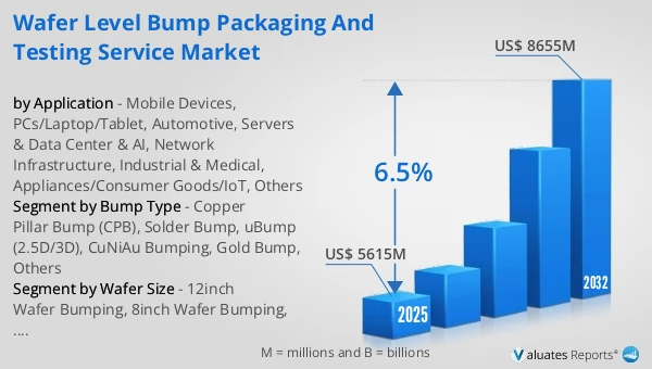
 Figure 36. Global Wafer Level Bump Packaging and Testing Service Production Value (US$ Million), 2021 vs 2025 vs 2032
 Figure 37. Global Wafer Level Bump Packaging and Testing Service Production Value (US$ Million), 2021–2032
 Figure 38. Global Wafer Level Bump Packaging and Testing Service Production Capacity (K Wafers), 2021–2032
 Figure 39. Global Wafer Level Bump Packaging and Testing Service Production (K Wafers), 2021–2032
 Figure 40. Global Wafer Level Bump Packaging and Testing Service Average Price (US$/Wafer), 2021–2032
 Figure 41. Wafer Level Bump Packaging and Testing Service Report Years Considered
 Figure 42. Wafer Level Bump Packaging and Testing Service Production Share by Manufacturers in 2025
 Figure 43. Global Wafer Level Bump Packaging and Testing Service Production Value Share by Manufacturers (2025)
 Figure 44. Wafer Level Bump Packaging and Testing Service Market Share by Company Type (Tier 1, Tier 2, and Tier 3): 2021 vs 2025
 Figure 45. Top 5 and Top 10 Global Players: Market Share by Wafer Level Bump Packaging and Testing Service Revenue in 2025
 Figure 46. Global Wafer Level Bump Packaging and Testing Service Production Value by Region: 2021 vs 2025 vs 2032 (US$ Million)
 Figure 47. Global Wafer Level Bump Packaging and Testing Service Production Value Market Share by Region: 2021 vs 2025 vs 2032
 Figure 48. Global Wafer Level Bump Packaging and Testing Service Production Comparison by Region: 2021 vs 2025 vs 2032 (K Wafers)
 Figure 49. Global Wafer Level Bump Packaging and Testing Service Production Market Share by Region: 2021 vs 2025 vs 2032
 Figure 50. North America Wafer Level Bump Packaging and Testing Service Production Value (US$ Million) Growth Rate (2021–2032)
 Figure 51. Europe Wafer Level Bump Packaging and Testing Service Production Value (US$ Million) Growth Rate (2021–2032)
 Figure 52. China Wafer Level Bump Packaging and Testing Service Production Value (US$ Million) Growth Rate (2021–2032)
 Figure 53. Japan Wafer Level Bump Packaging and Testing Service Production Value (US$ Million) Growth Rate (2021–2032)
 Figure 54. South Korea Wafer Level Bump Packaging and Testing Service Production Value (US$ Million) Growth Rate (2021–2032)
 Figure 55. Southeast Asia Wafer Level Bump Packaging and Testing Service Production Value (US$ Million) Growth Rate (2021–2032)
 Figure 56. China Taiwan Wafer Level Bump Packaging and Testing Service Production Value (US$ Million) Growth Rate (2021–2032)
 Figure 57. Global Wafer Level Bump Packaging and Testing Service Consumption by Region: 2021 vs 2025 vs 2032 (K Wafers)
 Figure 58. Global Wafer Level Bump Packaging and Testing Service Consumption Market Share by Region: 2021 vs 2025 vs 2032
 Figure 59. North America Wafer Level Bump Packaging and Testing Service Consumption and Growth Rate (K Wafers), 2021–2032
 Figure 60. North America Wafer Level Bump Packaging and Testing Service Consumption Market Share by Country (2021–2032)
 Figure 61. U.S. Wafer Level Bump Packaging and Testing Service Consumption and Growth Rate (K Wafers), 2021–2032
 Figure 62. Canada Wafer Level Bump Packaging and Testing Service Consumption and Growth Rate (K Wafers), 2021–2032
 Figure 63. Europe Wafer Level Bump Packaging and Testing Service Consumption and Growth Rate (K Wafers), 2021–2032
 Figure 64. Europe Wafer Level Bump Packaging and Testing Service Consumption Market Share by Country (2021–2032)
 Figure 65. Germany Wafer Level Bump Packaging and Testing Service Consumption and Growth Rate (K Wafers), 2021–2032
 Figure 66. France Wafer Level Bump Packaging and Testing Service Consumption and Growth Rate (K Wafers), 2021–2032
 Figure 67. U.K. Wafer Level Bump Packaging and Testing Service Consumption and Growth Rate (K Wafers), 2021–2032
 Figure 68. Italy Wafer Level Bump Packaging and Testing Service Consumption and Growth Rate (K Wafers), 2021–2032
 Figure 69. Russia Wafer Level Bump Packaging and Testing Service Consumption and Growth Rate (K Wafers), 2021–2032
 Figure 70. Asia Pacific Wafer Level Bump Packaging and Testing Service Consumption and Growth Rate (K Wafers), 2021–2032
 Figure 71. Asia Pacific Wafer Level Bump Packaging and Testing Service Consumption Market Share by Region (2021–2032)
 Figure 72. China Wafer Level Bump Packaging and Testing Service Consumption and Growth Rate (K Wafers), 2021–2032
 Figure 73. Japan Wafer Level Bump Packaging and Testing Service Consumption and Growth Rate (K Wafers), 2021–2032
 Figure 74. South Korea Wafer Level Bump Packaging and Testing Service Consumption and Growth Rate (K Wafers), 2021–2032
 Figure 75. China Taiwan Wafer Level Bump Packaging and Testing Service Consumption and Growth Rate (K Wafers), 2021–2032
 Figure 76. Southeast Asia Wafer Level Bump Packaging and Testing Service Consumption and Growth Rate (K Wafers), 2021–2032
 Figure 77. India Wafer Level Bump Packaging and Testing Service Consumption and Growth Rate (K Wafers), 2021–2032
 Figure 78. Latin America, Middle East & Africa Wafer Level Bump Packaging and Testing Service Consumption and Growth Rate (K Wafers), 2021–2032
 Figure 79. Latin America, Middle East & Africa Wafer Level Bump Packaging and Testing Service Consumption Market Share by Country (2021–2032)
 Figure 80. Mexico Wafer Level Bump Packaging and Testing Service Consumption and Growth Rate (K Wafers), 2021–2032
 Figure 81. Brazil Wafer Level Bump Packaging and Testing Service Consumption and Growth Rate (K Wafers), 2021–2032
 Figure 82. Israel Wafer Level Bump Packaging and Testing Service Consumption and Growth Rate (K Wafers), 2021–2032
 Figure 83. GCC Countries Wafer Level Bump Packaging and Testing Service Consumption and Growth Rate (K Wafers), 2021–2032
 Figure 84. Global Production Market Share of Wafer Level Bump Packaging and Testing Service by Package Technology (2021–2032)
 Figure 85. Global Production Value Market Share of Wafer Level Bump Packaging and Testing Service by Package Technology (2021–2032)
 Figure 86. Global Wafer Level Bump Packaging and Testing Service Price (US$/Wafer) by Package Technology (2021–2032)
 Figure 87. Global Production Market Share of Wafer Level Bump Packaging and Testing Service by Application (2021–2032)
 Figure 88. Global Production Value Market Share of Wafer Level Bump Packaging and Testing Service by Application (2021–2032)
 Figure 89. Global Wafer Level Bump Packaging and Testing Service Price (US$/Wafer) by Application (2021–2032)
 Figure 90. Wafer Level Bump Packaging and Testing Service Value Chain
 Figure 91. Channels of Distribution (Direct Vs Distribution)
 Figure 92. Bottom-up and Top-down Approaches for This Report
 Figure 93. Data Triangulation
SELECT A FORMAT
Added to Cart
Electronic

$2900

Single User License
Electronic

$4350

Multi User License
Electronic

$5800

Enterprise License
Add to Cart
Buy Now (15% Discount)

OUR CUSTOMER

Accenture