FEATURED COMPANIES
Unimicron
IBIDEN
Nan Ya PCB
AT&S
Kinsus Interconnect Technology
Kyocera
Toppan
Zhen Ding Technology
Daeduck Electronics
ASE Material
Flip-Chip Package Substrate Market Size
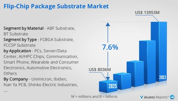
The global Flip-Chip Package Substrate market was valued at US$ 8036 million in 2025 and is anticipated to reach US$ 13953 million by 2032, at a CAGR of 7.6% from 2026 to 2032.
Flip-Chip Package Substrate Market
The 2025 U.S. tariff policies introduce profound uncertainty into the global economic landscape. This report critically examines the implications of recent tariff adjustments and international strategic countermeasures on Flip-Chip Package Substrate competitive dynamics, regional economic interdependencies, and supply chain reconfigurations.
A Flip-Chip Package Substrate (flip-chip package substrate / IC substrate for flip-chip) is the high-density interconnect structure between a flip-chipped die and the system PCB, providing I/O fan-out, power/ground distribution, high-speed routing, mechanical support, and a controlled path for thermal conduction. In industry practice, the most common product families are FC-BGA substrates (for CPUs/GPUs/AI accelerators, networking ASICs and other large, high-I/O packages) and FC-CSP substrates (for mobile processors, RF front-end modules and compact SiP platforms). The dominant construction is the organic build-up substrate, and Ajinomoto explicitly positions ABF as an essential material for forming the multi-layer “CPU bed” that connects nanometer-scale die terminals to millimeter-scale board-level terminals, enabled by laser processing and direct copper plating. FC-BGA substrates are also commonly defined as high-density semiconductor package substrates enabling high-speed, high-function LSI chips.
Flip-chip substrate manufacturing is a tightly coupled stack of organic build-up dielectrics + microvias + fine-line copper patterning + plating chemistry, executed on panel formats at high volume. ABF (and related films) are laminated as build-up layers; microvias are laser-drilled; vias are cleaned/desmeared and conditioned; copper is deposited (electroless + electrolytic) and patterned via SAP/mSAP and imaging to achieve high wiring density and multi-layer interconnect; then solder mask, surface finishes, cavity formation, backside metallization, and flatness/warpage controls are integrated to meet assembly windows. Ajinomoto highlights ABF’s continued evolution to meet CPU thermal stability and plating/laser-process requirements, underscoring how material/process co-optimization is central to this industry. SEMI-published process material for advanced packaging and IC-substrate manufacturing illustrates panel flows where via cleaning, adhesion/seed PVD (e.g., Ti/Cu), and subsequent plating (RDL/UBM) are key steps, while particle control, uniformity and warpage at larger panel sizes become yield-critical constraints.
The competitive landscape is multi-tiered: ABF and other dielectric suppliers at the material layer, a concentrated set of advanced IC-substrate makers at the manufacturing layer, plus equipment and wet-chemistry ecosystems, all co-optimizing with OSATs and system houses around performance and manufacturability. Market dynamics are increasingly shaped by AI/HPC and heterogeneous integration, which push larger package sizes, higher I/O density, tighter signal-integrity budgets, and higher power delivery/thermal demands. SEMI’s public exposition notes that demand for advanced substrates is forecast to rise exponentially and that scarcity has already appeared on the supply side, while highlighting technical directions such as embedded passives/actives, cavity structures for thinning/shielding, multifunctional cores for power delivery, and finer lines/smaller vias for advanced interconnect. Technology trends therefore include (i) continued UHDI scaling (fine-line SAP and robust microvia stacks) and (ii) structural/material innovations to address warpage and scaling limits—most notably glass-core / glass-material package substrate cores for better flatness and thermo-mechanical stability at large form factors. Samsung Electro-Mechanics publicly states it is developing glass-core package substrates and expects growth in high-end server CPUs and AI accelerators. AT&S similarly frames fine-line SAP and high-reliability microvia stacks as enabling massive pin-count escape routing without exploding layer counts or package footprints.
This report delivers a comprehensive overview of the global Flip-Chip Package Substrate market, with both quantitative and qualitative analyses, to help readers develop growth strategies, assess the competitive landscape, evaluate their position in the current market, and make informed business decisions regarding Flip-Chip Package Substrate. The Flip-Chip Package Substrate market size, estimates, and forecasts are provided in terms of output/shipments (Sqm) and revenue (US$ millions), with 2025 as the base year and historical and forecast data for 2021–2032.
The report segments the global Flip-Chip Package Substrate market comprehensively. Regional market sizes by Type, by Application, by Material, and by company are also provided. For deeper insight, the report profiles the competitive landscape, key competitors, and their respective market rankings, and discusses technological trends and new product developments.
This report will assist Flip-Chip Package Substrate manufacturers, new entrants, and companies across the industry value chain with information on revenues, production, and average prices for the overall market and its sub-segments, by company, by Type, by Application, and by region.
Market Segmentation
Scope of Flip-Chip Package Substrate Market Report
| Report Metric |
Details |
| Report Name |
Flip-Chip Package Substrate Market |
| Accounted market size in 2025 |
US$ 8036 million |
| Forecasted market size in 2032 |
US$ 13953 million |
| CAGR |
7.6% |
| Base Year |
2025 |
| Forecasted years |
2026 - 2032 |
| Segment by Type |
- FCBGA Substrate
- FCCSP Substrate
|
| Segment by Material |
- ABF Substrate
- BT Substrate
|
| by Application |
- PCs
- Server/Data Center
- AI/HPC Chips
- Communication
- Smart Phone
- Wearable and Consumer Electronics
- Automotive Electronics
- Others
|
| Production by Region |
- Japan
- South Korea
- China Taiwan
- China Mainland
|
| Consumption by Region |
- North America (United States, Canada)
- Europe (Germany, France, UK, Italy, Russia)
- Asia-Pacific (China, Japan, South Korea, Taiwan)
- Southeast Asia (India)
- Latin America (Mexico, Brazil)
|
| By Company |
Unimicron, Ibiden, Nan Ya PCB, Shinko Electric Industries, Kinsus Interconnect Technology, AT&S, Samsung Electro-Mechanics, Kyocera, Toppan, Zhen Ding Technology, Daeduck Electronics, Zhuhai Access Semiconductor, LG InnoTek, Shennan Circuit, Shenzhen Fastprint Circuit Tech, Korea Circuit, FICT LIMITED, AKM Meadville, Shenzhen Hemei Jingyi Semiconductor Technology, Simmtech, HOREXS, ASE Material, AaltoSemi |
| Forecast units |
USD million in value |
| Report coverage |
Revenue and volume forecast, company share, competitive landscape, growth factors and trends |
Chapter Outline
- Chapter 1: Defines the scope of the report and presents an executive summary of market segments (by Type, by Application, by Material, etc.), including the size of each segment and its future growth potential. It offers a high-level view of the current market and its likely evolution in the short, medium, and long term.
- Chapter 2: Provides a detailed analysis of the competitive landscape for Flip-Chip Package Substrate manufacturers, including prices, production, value-based market shares, latest development plans, and information on mergers and acquisitions.
- Chapter 3: Examines Flip-Chip Package Substrate production/output and value by region and country, providing a quantitative assessment of market size and growth potential for each region over the next six years.
- Chapter 4: Analyzes Flip-Chip Package Substrate consumption at the regional and country levels. It quantifies market size and growth potential for each region and its key countries, and outlines market development, outlook, addressable space, and national production.
- Chapter 5: Analyzes market segments by Type, covering the size and growth potential of each segment to help readers identify “blue ocean” opportunities.
- Chapter 6: Analyzes market segments by Application, covering the size and growth potential of each segment to help readers identify “blue ocean” opportunities in downstream markets.
- Chapter 7: Profiles key players, detailing the fundamentals of major companies, including product production/output, value, price, gross margin, product portfolio/introductions, and recent developments.
- Chapter 8: Reviews the industry value chain, including upstream and downstream segments.
- Chapter 9: Discusses market dynamics and recent developments, including drivers, restraints, challenges and risks for manufacturers, U.S. Tariffs and relevant policy analysis.
- Chapter 10: Summarizes the key findings and conclusions of the report.
FAQ for this report
How fast is Flip-Chip Package Substrate Market growing?
Ans: The Flip-Chip Package Substrate Market witnessing a CAGR of 7.6% during the forecast period 2026-2032.
What is the Flip-Chip Package Substrate Market size in 2032?
Ans: The Flip-Chip Package Substrate Market size in 2032 will be US$ 13953 million.
Who are the main players in the Flip-Chip Package Substrate Market report?
Ans: The main players in the Flip-Chip Package Substrate Market are Unimicron, Ibiden, Nan Ya PCB, Shinko Electric Industries, Kinsus Interconnect Technology, AT&S, Samsung Electro-Mechanics, Kyocera, Toppan, Zhen Ding Technology, Daeduck Electronics, Zhuhai Access Semiconductor, LG InnoTek, Shennan Circuit, Shenzhen Fastprint Circuit Tech, Korea Circuit, FICT LIMITED, AKM Meadville, Shenzhen Hemei Jingyi Semiconductor Technology, Simmtech, HOREXS, ASE Material, AaltoSemi
What are the Application segmentation covered in the Flip-Chip Package Substrate Market report?
Ans: The Applications covered in the Flip-Chip Package Substrate Market report are PCs, Server/Data Center, AI/HPC Chips, Communication, Smart Phone, Wearable and Consumer Electronics, Automotive Electronics, Others
What are the Type segmentation covered in the Flip-Chip Package Substrate Market report?
Ans: The Types covered in the Flip-Chip Package Substrate Market report are FCBGA Substrate, FCCSP Substrate